- News
28 September 2011
Improving etch process control in InGaN laser diodes
University of California Santa Barbara (UCSB), together with Japan’s Mitsubishi Chemical Corp, have developed an etch technique to produce more accurate ridge waveguides in nitride semiconductor laser diodes (LDs) [Robert M. Farrell et al, Appl. Phys. Express, vol4, p092105, 2011]. The technique uses an etch-stop layer of aluminum gallium nitride (AlGaN), and is made possible by UCSB’s development last year (UCSB achieves CW operation of AlGaN-cladding-free nonpolar lasers) of nitride LDs that do not use AlGaN for the thick cladding layers needed to confine optical modes in the structure.
Commercial indium gallium nitride/gallium nitride (InGaN/GaN) laser diodes are typically produced with ridge waveguides that need to be etched with accurate dimensions to enable stable, kink-free operation at high output power. However, existing etch methods in nitride semiconductors do not deliver the depth control needed for accuracy, reproducibility, and hence good device yields.
The purpose of ridge waveguides in laser diodes is to laterally confine the optical modes in the structure: too shallow, and optical confinement is lost and current spreading can occur, reducing injection efficiency; too deep, and higher-order modes of the cavity become dominant, leading to unstable far-field patterns and kinks in the light output power-current (L-I) performance. Sometimes the ridge can be etched right through to the active layers where surface recombination states can be set up, decreasing device lifetimes.
One technique for increased etch-depth control used in other material systems (e.g. gallium arsenide, indium phosphide) is to have an etch-stop layer through which the chosen etch method slows considerably. Such selective etching has been applied to nitride semiconductor high-electron-mobility transistors (HEMTs).
Unfortunately, one potential etch-stop material, aluminum gallium nitride (AlGaN), is used as cladding in existing InGaN/GaN LDs, precluding its use in this context. However, UCSB, and separately a Swiss consortium (EPFL, NovaGaN, Exalos), have developed nitride LDs with AlGaN-free cladding structures, which would allow the use of such etch-stop techniques.
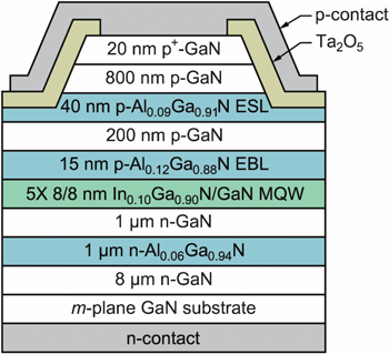 Metal-organic chemical vapor deposition (MOCVD) was used to create laser diode structures (Figure 1) on free-standing m-plane GaN substrates supplied by Mitsubishi. The substrates had a deliberate misorientation of 1° toward the [000-1] c-direction to improve the crystal growth quality. The epitaxial structures for one sample (A) contained electron-blocking (EBL) and etch-stop (ESL) layers. Another sample (B) consisted of 8μm of n-GaN, as a reference for the etch rate experiments. The dry etching was performed in a Panasonic E620 inductive coupled plasma system. The plasma consisted of a mix of boron trichloride and sulfur hexafluoride.
Figure 1: Cross-sectional schematic of LD based on sample A.
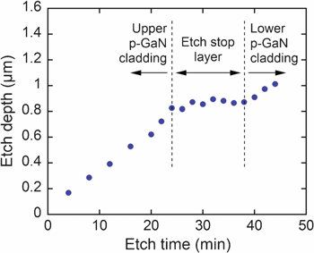 The researchers estimate that the etch process proceeded through GaN at the rate of 31.6nm/min (Figure 2). This compares with the rate found for the AlGaN ESL etch of 2.9nm/min, giving a GaN:AlGaN selectivity of 11:1. The researchers performed a 30-minute mesa etch for an LD ridge on co-loaded samples A and B, which gave etch depths of 0.86μm and 1.03μm, respectively. The lower value for sample A indicates that the AlGaN was successful in stopping the etch at the appropriate point.
Figure 2: Dependence of etch depth on time for sample A.
Diodes produced from sample A had threshold voltages and currents of 9.7V and 210mA, respectively. The researchers comment that the threshold current density of 10.5kA/cm2 was “relatively high”, compared with similar device structures. However, they hope for improvements with further optimization. In terms of spectrum, the peak shifted to longer wavelengths at higher currents (red shift) with a peak wavelength of 399.9nm (ultraviolet) and full-width at half-maximum (FWHM) of 1.1nm at 300mA.
Funding support for the research came from Solid State Lighting and Energy Center (SSLEC), based at UCSB, and the Visible InGaN Injection Laser (VIGIL) program, run by US Defense Advanced Research Projects Agency (DARPA)
Low threshold for m-plane nitride semiconductor lasing
Yet another angle on nitride laser diodes
AlGaN-cladding-free semipolar laser nears green
The author Mike Cooke is a freelance technology journalist who has worked in the semiconductor and advanced technology sectors since 1997.