- News
26 September 2011
Current spreading for higher nitride LED output power
Taiwan National Central University researchers have used two-dimensional electron gas (2DEG) layers in the n-type region of nitride light-emitting device to improve current spreading [Hsueh-Hsing Liu et al, IEEE Electron Device Letters, published online 30 August 2011]. This resulted in lower forward voltages, and higher output power and wall-plug efficiency.
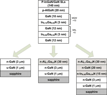 Three device structures were grown for comparison on c-plane sapphire using metal-organic chemical vapor deposition (MOCVD) — see Figure 1. The devices differed in having layers inserted between the n-GaN buffer layer and the subsequent stack of active and p-contact layers. This stack included a five-period strain-reducing layer (SRL), p-Al0.1Ga0.9N electron-blocking layer (EBL), and modulation-doped p-GaN/InGaN superlattice p-contact. The p-type doping was achieved using magnesium.
Figure 1: Layer structures of the LEDs investigated.
The epitaxial structures were processed into 1mm x 1mm LEDs with indium tin oxide (ITO) alloy transparent conducting layers on the p-contact.
The three LED n-layer current spreading insertions were: none (LED A); one n-AlGaN layer (LED B); and three layers consisting of n-InGaN, n-GaN, and n-AlGaN (LED C). The extra layers, if present, were designed to improve lateral current spreading through the LED structure. Transmission line method (TLM) measurements on epitaxial structures, without the subsequent LED structures, gave sheet resistances for the LED n-type bases of 50Ω/square (A), 20Ω/square (B), and 10Ω/square (C).
The increase in conductivity in structures B and C arose from the presence of 2DEGs at the n-AlGaN/n-GaN and n-GaN/n-InGaN interfaces due to the polarization field differences between the respective materials. Such 2DEGs are used in nitride high-electron-mobility transistors (HEMTs).
LED B had one 2DEG due to spontaneous polarization and LED C had two due to both spontaneous (n-AlGaN/n-GaN) and strain-dependent piezoelectric (n-GaN/n-InGaN) polarization. Simulations suggest that the AlGaN/GaN 2DEGs had carrier densities of ~2x10¹⁹/cm2 and the GaN/InGaN 2DEG had a carrier density of ~4x10¹⁹/cm2, “consistent” with the TLM results.
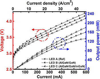 The simulation shows a potential drawback from including AlGaN in the n-type layers as being a raised barrier to electron injection into the active light-emitting layers. In fact, the forward voltage of the devices at 350mA was found experimentally (Figure 2) to be reduced in LEDs B and C due to the better current spreading under the active region: 3.84V for LED A (normal device), 3.76V for LED B, and 3.67V for LED C.
Figure 2: Output powers and forward voltages of LEDs A, B, and C under CW operation. LED C, which has an n-Al0.1Ga0.9N/GaN/In0.06Ga0.94N current-spreading layer, exhibits the highest output power and lowest forward voltage compared with LEDs A and B.
The output powers of these devices at 350mA injection current were 109mW, 118mW and 129mW, for LEDs A–C, respectively. The output power of C was increased by 18% over A. The increase in wall-plug efficiency was 22%, giving a lower junction temperature in C. The variation in light emission across the three devices was measured at 32%, 24% and 21%, for LEDs A–C, respectively.
The researchers believe these improvements in performance could be carried over to devices with optimized thickness and doping level and/or multiple stacks of the heterostructure current spreading layer.
Tekcore Company assisted in device processing and professor Y-R Wu of the National Taiwan University performed device simulations for the research.
The author Mike Cooke is a freelance technology journalist who has worked in the semiconductor and advanced technology sectors since 1997.