- News
7 September 2011
EQE increased 2.4-fold with void-embedded cortex nano-patterned LED
Taiwan-based researchers have developed a sapphire nanopatterning technique that increases external quantum efficiencies (EQE) of nitride semiconductor LEDs by 2.4x over devices grown on conventional sapphire at 20mA drive current [Yu-Sheng Lin and J. Andrew Yeh, Appl. Phys. Express, vol4, p092103, 2011].
The researchers at National Tsing Hua University and National Applied Research Laboratories comment that the EQE of 58.3% at 20mA is comparable with that of other reported devices on nanopatterned sapphire substrates with values in the range 40–50%. The conventional device had an EQE of 24.5%. The output power measured from the top side of the devices at 20mA was 33.1mW for the patterned device and 13.9mW for the conventional LED.
Many researchers are seeking low-cost ways to enhance the performance of nitride semiconductor LEDs. One technique for this has been to pattern the sapphire substrate used before nitride growth. These nano-scale patterns can have two effects to improve the performance of the resulting LEDs.
First, the nanopatterned surface affects the growth process, reducing the number of dislocations in the nitride semiconductor crystal; such dislocations can degrade LED performance. Second, the growth process often creates air-voids at the interface between the sapphire and nitride semiconductor heterostructure; the voids can be used to alter the way the light generated by the LED action leaves the device. Sometimes both effects operate to improve EQEs of nitride LEDs.
The Taiwan researchers used a random nanopatterning that they called ‘void-embedded cortex-like nanostructures’ (VECN). The team sees their method as being “a cost-effective solution to the wafer-level cortex-like nanostructures on sapphire for high-efficiency LEDs without implementation of an expensive semiconductor mask”.
The nanopatterning of the sapphire wafer surface was achieved by creating a 2μm-thick hard mask of polysilicon and performing an inductively coupled plasma reactive-ion etch with a boron tetrachloride and chlorine mix. The deposition of the polysilicon was through 640°C low-pressure chemical vapor deposition. The patterning for the hard mask was created by dipping the polysilicon-covered wafer in diluted Wright-etch solution for 30 minutes. Wright-etch solution is an acid mix developed in the 1970s to reveal defects in silicon crystal structures. The hard mask was removed by potassium hydroxide solution at 80°C. The resulting patterning of the sapphire wafer surface consisted of 1010/cm2 80–150nm deep structures spaced 50–150nm apart (Figure 1).
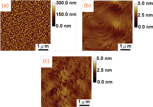
Figure 1: AFM images of surfaces of (a) sapphire with void-embedded cortex-like nanostructure (VECN), (b) undoped gallium nitride (u-GaN) on VECN sapphire, and (c) u-GaN on conventional sapphire. Scan area is 5μm x 5μm.
The LED structures were grown using low-pressure metal-organic chemical vapor deposition (Figure 2). Atomic force microscopy (AFM) of the buffer layer suggested a pit density of 107–108/cm2. This is two orders of magnitude lower than pit density values for gallium nitride (GaN) grown on conventional sapphire substrates (CSS). Such pits are attributed to threading dislocations that propagate from the sapphire to the top of the GaN surface.
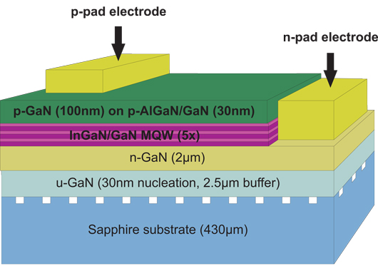
Figure 2: Schematic diagram of LED-VECN structure. The p-side layers consist of 30nm aluminum gallium nitride/gallium nitride (AlGaN/GaN) superlattice and 100nm p-GaN.
X-ray diffraction (0002) rocking curve full-width at half maximum (FWHM) values of 211 arcsec for the nanopatterned GaN/sapphire, compared with 294 arcsec for GaN/CSS, also suggest improved crystal quality. The further LED layers slightly increased the FWHM for the nanopatterned device structure to 216 arcsec, while the CSS device structure FWHM decreased to 256 arcsec. Satellite peaks up to fifth order were detected, suggesting good layer periodicity for the indium gallium nitride/gallium nitride (InGaN/GaN) multi-quantum wells (MQW), which made up the active region of the device.
The electroluminescent peak occurred at 438nm (violet) at 20mA drive current (Figure 3). At 20mA, the patterned LED had a lower forward voltage of 3.6V, compared with the conventional device’s 3.8V. The reflection from the GaN/sapphire interface was 32.8% higher in the patterned device compared with that on conventional sapphire. The reflection is thought to occur at air voids formed during the GaN growth. Such reflection occurs due to the large difference in refractive index between GaN (2.45) and air (~1).
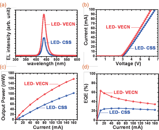
Figure 3: (a) Electroluminescence spectra for LED on VECN and conventional (CSS) substrate located at 438nm under an injection current of 20mA. (b) Current–voltage (I–V) curves of the LED-VECN and the LED-CSS, (c) light output power, and (d) EQE in relation to current characteristics of LED-VECN and LED-CSS, respectively.
The characterizations of the crystal structure and light reflection suggest that the improvement results from both reduction in dislocation density, and improved light extraction through reflection.
Nano-patterned LEDs AlGaN/GaN Sapphire substrates
The author Mike Cooke is a freelance technology journalist who has worked in the semiconductor and advanced technology sectors since 1997.