- News
4 October 2011
Graded refractive index structures boost LED emission by up to 131%
Researchers in the USA and South Korea have used patterned layers of titanium-silicon dioxide (TiO2/SiO2) dielectrics to enhance light output from indium gallium nitride (InGaN) light-emitting diodes (LEDs) by up to 131% [Ahmed N. Noemaun et al, J. Appl. Phys., vol110, p054510, 2011].
The layers work by stepping down the refractive index of the material through which light passes from the high value of 2.47 for GaN to 1 for air. Patterning of the graded refractive index (GRIN) coating allows light to be extracted from the side walls of the dielectric structures.
In the absence of such dielectric layers the large difference in refractive index reduces the angles at which light can emerge from an GaN/air interface to within 24° to the surface normal. Light hitting at greater angles (24-90°) is reflected back into the device, a situation called total internal reflection (TIR).
The researchers from Rensselaer Polytechnic Institute, Samsung LED and Pohang University of Science and Technology developed the GRIN technology using 1mm x 1mm 445nm-wavelength nitride semiconductor LEDs grown on c-plane sapphire using metal-organic chemical vapor deposition (MOCVD). The LED layers were lifted-off the underlying sapphire substrate using a 248nm krypton fluoride excimer laser beam.
The separated GaN surface was a nitrogen-face. Two reference LED types consisted of devices with no passivation and planar GaN N-face, and devices with roughened surfaces created through wet etching with 10%-by-weight potassium hydroxide solution for 4 minutes at 50°C.
For the devices with GRIN structures, a series of layers with varying thickness and refractive index were applied by sputtering combinations of titanium (TiO2) and silicon (SiO2) dioxide (Table 1). The chamber pressure was 2mTorr and was subjected to a 10/0.5 standard cubic centimeter (sccm) flow of argon/oxygen. The substrate plasma was generated at 100V bias.
Layer number |
Power applied to TiO2 target |
Power applied to SiO2 target |
Deposition time |
Measured layer thickness |
Measured refractive index |
1 |
200W |
0W |
240min |
333nm |
2.47 |
2 |
200W |
50W |
180min |
331nm |
2.26 |
3 |
200W |
100W |
120min |
323nm |
1.99 |
4 |
200W |
150W |
90min |
330nm |
1.83 |
5 |
0W |
200W |
120min |
260nm |
1.46 |
Table 1: Thickness and refractive index of each layer in the graded-refractive-index stack is controlled by the power applied to the TiO2 and SiO2 targets and the deposition time.
 The GRIN layers were followed by a 127nm layer of indium tin oxide (ITO), which was used as the hard mask for the patterning of the GRIN layers. Photolithography was carried out using a Shipley S1813 photoresist and the pattern transferred to the ITO mask using a methane/hydrogen/chlorine inductively coupled plasma reactive ion etch (ICP-RIE). Having formed the hard mask, the TiO2-SiO2 layers were patterned with trifluoromethane (CHF3), again using ICP-RIE. The etch residues were removed using a 30 minute 80°C dip consisting of a photoresist stripper.
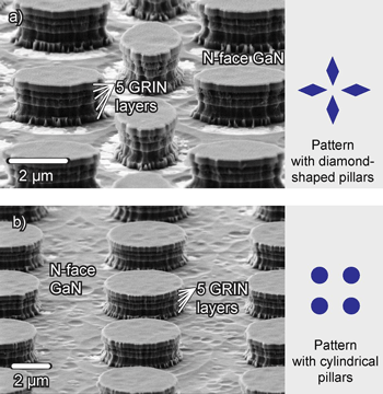
Figure 1: Scanning electron micrographs (SEMs) of (a) an array of diamond-shaped pillars and (b) an array of cylindrical pillars etched under 1kW ICP power and 400W RIE power with 60sccm of CHF3 at 15mTorr and 50°C.
The tilt angle of the resulting pillars of dielectric was less than 5°. The patterns were either cylindrical or diamond-shaped pillars (Figure 1). These patterns were designed using theoretical calculations involving ray tracing.
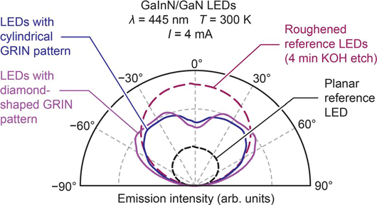
Figure 2: Far-field emission intensity of planar reference LEDs, KOH-roughened reference LEDs, LEDs with GRIN cylindrical patterns with 2μm diameter, and LEDs with GRIN diamond-shaped patterns with 4.7μm longer diagonal and 2μm shorter diagonal.
Although the patterning increased the forward voltage of the devices, improved light output up to 131% was achieved (Table 2). The planar and roughened far-field emission patterns are described as ‘Lambertian’, with peaks at 0°, while the emission for cylindrical and diamond patterned GRIN layers peaks at an off-surface normal direction between 25° and 55° (Figure 2). The researchers comment: “The strong side emission is consistent with our expectations resulting from theoretical calculations.”
Type |
Spacing |
Dimensions |
Improvement in light output |
Forward voltage |
Planar |
|
|
0% |
2.64V |
Roughened |
|
|
124% |
2.7V |
Cylinder GRIN |
2μm |
2μm diameter |
104% |
2.67V |
Diamond GRIN |
4μm |
2x4.7μm diagonals |
131% |
2.67V |
Table 2: Performance results for some of the devices compared at 4mA.
The researchers suggest that patterning of GRIN layers on LEDs could also be used “to convert trapped modes of light inside a semiconductor into designable modes with desirable properties, such as preferential direction of emission and polarization of light.”
Financial support came from a wide range of sources: Samsung LED Co, the Korean Ministry of Knowledge Economy through International Collaborative R&D Program, and the USA’s Sandia National Laboratories, National Science Foundation, Department of Energy, Department of Defense, NY State Energy Research and Development Authority (NYSERDA), Magnolia Solar Inc, and Raydex Technology Inc.
The author Mike Cooke is a freelance technology journalist who has worked in the semiconductor and advanced technology sectors since 1997.