- News
17 November 2011
First e-mode AlInN/GaN MOS-HFET using SiON insulation
Nitek Inc and University of South Carolina (USC) have reported the first enhancement-mode (normally-off) aluminum indium nitride on gallium nitride (AlInN/GaN) metal-oxide-semiconductor heterostructure field-effect transistors (MOS-HFETs) using silicon oxynitride (SiON) as the gate insulator [Daniel Morgan et al, Appl. Phys. Express, vol4, p114101, 2011].
A 1.5μm gate-length device with 8μm source–drain spacing demonstrated a positive threshold voltage of about 1.8V and a maximum dc output current density of 0.7A/mm. Three-terminal off-state (0V gate potential) breakdown occurred at 345V.
“The results of this study clearly show the potential of normally-off AlInN-GaN MOS-HFETs as next-generation devices for the realization of power electronics systems,” the researchers say.
Normal nitride semiconductor HFETs use a Schottky metal-semiconductor contact. These devices have a negative threshold voltage and are therefore normally ‘on’ with zero gate potential (depletion-mode operation). For many applications, normally-off/enhancement-mode operation is desired to reduce power consumption and for failure protection.
Special processing and structuring can achieve normally-off behavior, but usually some performance factor is adversely affected, such as on-resistance, off-state breakdown voltage, threshold voltage or on-state drain current.
Metal-insulator-semiconductor aluminum gallium nitride/gallium nitride (AlGaN/GaN) devices have shown some promise, with Fujitsu achieving output currents of 800mA/mm, with a threshold of +3V and breakdown at 320V.
Recently high-quality AlInN has been developed and used instead of AlGaN as the barrier layer to provide higher charge density in the channel near the GaN interface. This higher charge is induced by spontaneous polarization fields in the nitride material. Higher charge densities give the potential of higher conductance, and hence lower resistance current flow.
 Another advantage of high-quality AlInN is that the proportions of Al and In can be balanced to give layers that are lattice matched to GaN, unlike AlGaN that is always strained in tension. This balance is achieved at around 17% In (83% Al). Lattice matching improves material quality by avoiding strain-generated defects.
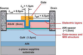
Figure 1: Schematic cross-section of the AlInN/AlN/GaN MOS-HEMT with a recessed-gate geometry and SiON gate dielectric. The gate–drain distance is 4.5μm and the total channel length is 8μm.
The Nitek/USC devices (Figure 1) were grown on sapphire substrates using metal-organic chemical vapor deposition (MOCVD). The deposition began with a 300nm lattice-matched aluminum nitride (AlN) layer. The AlInN/AlN/GaN layer structure resulted in an epitaxial material with room-temperature sheet carrier density of 2.1x10¹³/cm2, mobility of 1338cm2/V-s, and sheet resistance of 204Ω/square.
The MOS-HFETs were created on isolated mesas. The ohmic source–drain contact resistance for the non-optimized titanium-based metal stack was 0.7Ω-mm.
Silicon nitride (SiN) passivation was deposited using plasma-enhanced CVD. The gate region was first defined by etching a 1.8μm ‘long’ (i.e. in the plane of Figure 1) trench in the SiN that was 100μm ‘wide’ (perpendicular to plane). This etch process revealed the AlInN surface. The trench was continued down to the AlN with a controlled, low-power boron trichloride-based reactive ion etch.
The gate recess was coated with ~30nm of silicon oxynitride (SiON) using a ‘digital oxide deposition’ (DOD) that consisted of alternate pulses of oxygen and nitrogen precursor in a plasma-enhanced CVD process. The DOD allows for smooth layers to be created with precise thickness control. The process was previously reported by USC for use with AlGaN/GaN HFETs in 2006.
The 1.5μm nickel/gold gate metal was then deposited asymmetrically between the source and drain contact regions with a source–gate distance of about 2μm. No passivation was added after the gate was defined.
The maximum saturation current density of 0.5A/mm for the devices was reached at a gate voltage of 4V. At 6V gate potential, the drain current was 0.7A/mm.
The MOS-HFET devices operated in normally-off/enhancement mode with a threshold voltage of +1.5–2.0V. By contrast, a comparison device with conventional Schottky gate HFET had a negative threshold (–2.3V) giving normally-on/depletion behavior. The 4V shift in threshold is attributed to barrier layer thinning and insertion of a relatively thick dielectric layer between gate and channel.
The MOS-HFETs generally had a drain current leakage of 1mA/mm with 0V gate ‘off-state’, although for some devices the value was as high at 33mA/mm. The 0V-gate current was attributed to leakage through the GaN buffer.
The peak extrinsic transconductance of the MOS-HFET was 272mS/mm, compared with 200mS/mm for the traditional HFET. The researchers note that the transconductance is higher in the MOS-HEMT despite the 30nm-thick dielectric between the gate and channel.
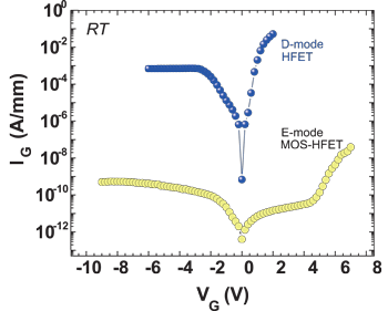 The impact of dielectric insulation on gate leakage currents is several orders of magnitude (Figure 2). Without dielectric, the conventional Schottky HFET has an appreciable increase in gate current above +2V, while the MOS-HFET can continue to operate beyond +5V with significantly less than 1μA/mm leakage. At +6V, the leakage is only 4.3nA/mm. Under reverse bias, the device had less than 550pA/mm leakage.
Figure 2: Gate-leakage current IG as a function of VG for insulating-gate E-mode MOS-HFET and conventional D-mode HFET.
The three-terminal breakdown characteristics were also investigated, where the both types of device were found to sustain 345V drain bias. The researchers believe that this value can be increased by dealing with buffer leakage effects and improving surface passivation. The devices were not immersed in 3M’s Fluorinert insulating cooling fluid, which is sometimes used in such measurements.
The work at Nitek Inc was supported by the US Missile Defense Agency.
The author Mike Cooke is a freelance technology journalist who has worked in the semiconductor and advanced technology sectors since 1997.