- News
22 November 2011
AlN interlayer doubles conversion of nitride semiconductor solar cell
Japan’s National Institute for Materials Science (NIMS) has used a super-thin layer of aluminum nitride (AlN) to double the conversion efficiency of nitride semiconductor photovoltaic solar cells [Liwen Sang et al, Appl. Phys. Lett., vol99, p161109, 2011].
The AlN is placed between the intrinsic/undoped indium gallium nitride (InGaN) active region and the p-contact layers. The researchers believe that the AlN acts both as an electron barrier for stopping leakage in forward and reverse bias, and as a block to growth of dislocations into the p-InGaN.
The nitride materials were grown on sapphire substrates using metal-organic chemical vapor deposition (MOCVD). The GaN template-buffer region was grown in a standard two-step process. Next, a 150nm layer of n-In0.15Ga0.85N was grown at a lowered temperature of 800°C, followed by an undoped 240nm-thick In0.15Ga0.85N active region.
The p-type layers were grown in two different ways. Sample A consisted of 90nm of p- In0.15Ga0.85N and 15nm of p-GaN. Sample B had an AlN interlayer (IL) before the same p-type layers (Figure 1 inset). The hole concentration for the p-InGaN was measured by Hall techniques as being 1.2x10¹⁸/cm3. The mobility was 2.6cm2/V-s.
The standard solar-cell devices were not enhanced with current-spreading layers or anti-reflective coatings.
One effect of the AlN interlayer is to reduce dark current (Figure 1) by two orders of magnitude (a factor of 100). At a reverse bias of –3V, the current density is 9.76x10⁻⁴A/cm2 without interlayer, but 4.72x10⁻⁶A/cm2 with.
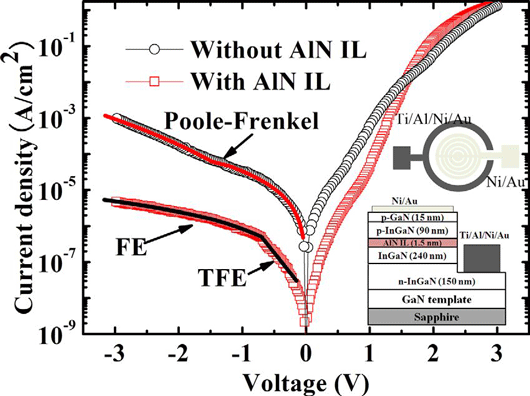
Figure 1: Dark current–voltage (I–V) characteristics of solar cell devices without (device A) and with (device B) AlN IL. Inset: structure of device with AlN IL and fabricated electrode configuration.
Other parameters, such as ideality and saturation current density, are also improved by including the interlayer. The ideality improvement from 6.0 (without IL) to 3.9 (with) is thought to result from better material quality across the p-n junction and reduced carrier tunneling.
Series resistance, estimated from the dark current–voltage curves, was slightly higher for the Al interlayer device (140Ω rather than 113Ω). This higher resistance may result from the presence of the interlayer itself.
The photovoltaic performance under 1.5 air mass (AM) simulated solar radiation showed increased performance (Table 1) such as a short-circuit current for sample B of 1.25mA/cm2, compared with 0.77mA/cm2 for sample A. The maximum power density for device B was 1.05mW/cm2, corresponding to a conversion efficiency of 1.05%. The conversion efficiency for the device without AlN interlayer was almost halved, at 0.55%.
Photovoltaic property |
Device A (without AlN IL) |
Device B (with AlN IL) |
Jsc (mA/cm2) |
0.77 |
1.25 |
Voc (V) |
1.31 |
1.50 |
Rsh (Ω-cm2) |
1.55x10⁴ |
1.96x10⁴ |
Rs (Ω-cm2) |
4.78x10² |
6.28x10² |
Fill factor (%) |
55 |
56 |
Conversion efficiency (%) |
0.55 |
1.05 |
Table 1: Summary of photovoltaic performance of samples.
The reduced shunt resistance of sample B is seen as indicating a reduction in bulk defects across the p-n junction. The open-circuit voltage is also improved by insertion of the AlN interlayer.
In terms of spectral performance, the peak external quantum efficiency of 50% was found at 372nm for device A, and more than 80% at the same wavelength for device B. Since the 372nm wavelength falls in the ultraviolet, the low conversion efficiency is no surprise, since the bulk of solar radiation comes in at wavelengths longer than around 500nm. There are hopes that active layers with higher indium content will bridge this gap, but such material becomes increasingly difficult to grow with high quality.
The researchers believe that the reverse bias leakage in device A is due to trap-assisted effects. The traps could arise from the greater density of structural defects across the p-n junction in this device structure. In device B, by contrast, the reverse leakage is restricted to thermionic field emission tunneling effects.
The researchers comment: “The different electrical transport mechanisms of these two devices imply that the structural defects are suppressed by the AlN layer in the p-InGaN layer.”
The researchers used transmission electron micrography (TEM) and atomic force microscopy (AFM) to study the defects. They found that the AlN layer blocked some of the screw-type dislocations from reaching the p-InGaN material.
The AFM study confirmed this, showing a reduced surface density of the V-pits that are associated with screw-type dislocations. According to the AFM study, the root-mean-square surface roughness was 1.1nm in sample B, but 2.1nm in sample A. Further, the AFM images show that sample A had grown with a spiral growth mode, whereas sample B had realized step-flow growth that indicates better quality p-InGaN.
Improving PV material quality with patterned sapphire
Superlattice nitride solar cells achieve higher conversion
Nitride solar cell AlN interlayer GaN InGaN MOCVD
The author Mike Cooke is a freelance technology journalist who has worked in the semiconductor and advanced technology sectors since 1997.