- News
19 November 2011
Graphite substrate exploration for vertical nitride LEDs
Korea’s universities have used aluminum-alloyed graphite as a thermally conducting substrate to improve the light output power performance of nitride semiconductor light-emitting diodes (LEDs) by 23% [H K Lee et al, Semicond. Sci. Technol., vol26, p115011, 2011]. Korea Advanced Nano-Fab Center (KANC) supported the device fabrication.
Conventional nitride semiconductor LEDs grown on sapphire are forced to use a lateral conduction scheme since the substrate is insulating. LEDs, particularly with nitrides, perform better with vertical conduction where the current density is uniform. This can be achieved by separating the nitride semiconductor from the sapphire substrate on which the device layers are grown.
Generally, the layers have to be transferred to a new substrate before separation. It is advantageous to choose substrates that are thermally conducting, since junction temperature is also important in LED performance. The Kyung Hee/Dongguk are exploring the graphite-based option as a low-cost alternative to the use of much more expensive replacement of sapphire by gallium nitride (GaN) or silicon carbide (SiC).
The blue (~450nm) indium gallium nitride (InGaN) LED structures were grown on 430μm thick sapphire substrates using metal-organic chemical vapor deposition (MOCVD). The undoped GaN buffer was 3.5μm, the n-GaN 4μm, and the p-GaN 0.21μm. The active region, sandwiched between the n- and p-GaN, consisted of five pairs of undoped InGaN/GaN layers, creating a multi-quantum well (MQW).
This material was then used to make both traditional lateral LEDs (LLEDs) and also vertical LEDs (VLEDs) through transfer/flipping onto 500μm-thick aluminum-alloyed graphite substrates (Figure 1). The aluminum alloy allows tuning of the thermal expansion coefficient. The final devices measured 1mm x 1mm.
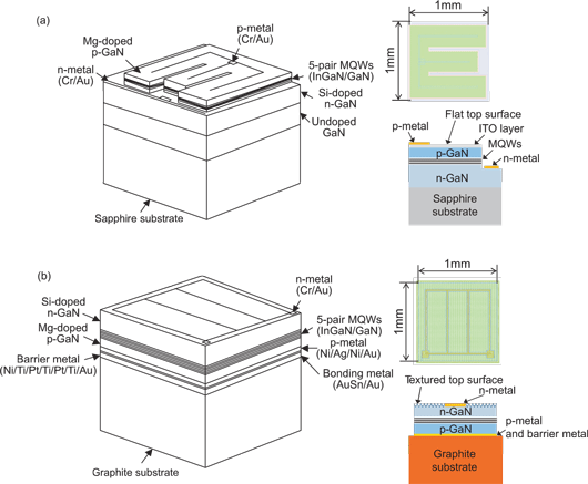
Figure 1: Schematic diagrams of fabricated GaN-based (a) LLED on sapphire substrate and (b) VLED on graphite substrate with mesa size of 1mm x 1mm.
The VLED process consisted of depositing p-contact and barrier metal layers on the p-GaN contact layer using e-beam evaporation. The barrier layer was needed to prevent tin (Sn) from the gold-tin/gold (AuSn/Au) graphite bond from diffusing into the LED.
The epitaxial layers were flipped and bonded to the graphite. The sapphire substrate layer was now removed using a 248nm krypton fluoride excimer laser lift-off process. The undoped GaN layer was etched away with an inductively coupled plasma. The n-GaN surface was roughened by immersion in potassium hydroxide solution for 15 minutes at 50°C to improve light extraction.
The LLEDs were processed in a conventional way with a 200nm indium tin oxide (ITO) current-spreading layer being deposited and annealed at 600°C for 1 minute, before mesa etching and metal contact deposition.
To enable temperature-dependent measurements (288–378K), the chips were indium-bonded to copper heat-sinks and wire-bonded to contact pads.
The light output powers for the LLED and VLED were 127.2mW and 156.4mW, respectively, at 350mA injection current and 298K temperature. The improved performance of the VLED is attributed to improved extraction from the surface roughening and the reflective metal layers at the base of the device. Such enhancements are difficult to implement in the LLED since the top layer of p-GaN is thin and there is a lack of reflectors to avoid light entering and being trapped in the sapphire substrate.
The far-field emission pattern was different for the two devices with the LLED having a wider beam due to light being emitted from all directions in the active layer. In the VLED, the bottom reflector is thought to increase extraction in the upward direction, giving a narrower, more directional beam.
Thermal measurements showed a gradual decrease in performance of the VLED at higher temperatures beyond 338K. Light output power in the range 288–338K was nearly constant at 156.4mW for an injection current of 350mA. This decreased to 149.4mW at 378K, a fall of 4.5%. The decrease became more significant at higher injection currents: at 700mA, the power values were 262.8mW and 236.6mW at 288K and 378K, respectively, a fall of 10%.
Temperature also affected turn-on and forward voltages. The turn-on voltage decreased with increasing temperature, being 2.65V at 288K and 2.39V at 378K. The forward voltages for a 350mA injection current were 3.84V at 288K and 3.47V at 378K.
Thermal degradation was more marked in the LLEDs on sapphire substrates, due to its lower thermal conductivity compared with the Al-graphite alloy. The decrease in light output power for the LLEDs in the range 288–378K is given as 12%. Fitting an exponential decrease to the fall in light emission intensity beyond 298K, the researchers derived characteristic temperatures (T1) of 295K and 414K for the LLED and VLED, respectively. The higher characteristic temperature for the VLED is indicative of the weaker dependence of its performance on temperature.
The impact of using a vertical current injection structure was also seen in a higher external quantum efficiency (EQE) of 16.2% at 350mA, compared with 13.2% for the LLED. At 550mA, the VLED EQE decreased 11.9%, compared with 14.6% for the LLED. Increasing the heat-sink temperature above 298K (~room temperature) decreases overall efficiency in these devices, but the degradation is slower for the VLED, compared with the LLED. For the temperature range 288–338K, the VLED maintained an approximately constant value with degradation only appearing beyond this. At 378K, the EQE for the VLED was 15.5% (–4.3%) for the VLED at 350mA injection.
A further effect of temperature increase is to narrow the energy gap, red-shifting the radiation to longer wavelengths. Between 298K and 378K, the peak wavelength of the LLED shifted from 449.3nm to 453.7nm (0.55nm/K), and the VLED from 449.5nm to 453.2nm (0.48nm/K). By contrast, there was a blue-shift in wavelengths as the current increased to 300mA, after which the wavelength remained constant in the VLED.
For the LLED, Joule heating in the devices due to the poor thermal conductivity of the sapphire substrate leads to red-shifting at currents beyond 300mA, because the real junction temperature is higher than that of the thermal stage that was used to control the temperature.
The initial blue-shift is attributed to the quantum-confined Stark effect (QCSE), where the changing electric field in the MQWs for different injection currents shifts the energy bands differently and hence affects the emission wavelength. The polarization fields that arise in nitride semiconductors due to spontaneous and piezoelectric (strain-dependent) effects tend to increase QCSEs.
The junction temperatures of the various devices at different injection currents in continuous wave (CW) operation were estimated through the initial forward and the voltage after 30 minutes, when the device had reached thermal equilibrium. The dependence of the forward voltage on temperature was estimated from pulsed measurements at controlled temperatures where thermal equilibrium of the junction is not reached.
In a 298K environment, the junction of the LLED reached 300.6K at 60mA and 312.4K at 350mA (40.74K/A increase). The same experiment on the VLED gave 299.7K and 310.2K (35.68K/A), respectively. The results suggest a thermal resistance of 10.12K/W for the VLED, compared with 12.53K/W for the LLED. Previous work by Kyung Hee University and Korea Advanced Nano Fab Center achieved ~8K/W for a VLED on 100μm copper. Three of the researchers from the new work were involved in this earlier result.
The researchers conclude that “the graphite substrate can be considered as a promising candidate for high-brightness LEDs by the wafer bonding process.”
Blue LEDs Graphite substrates GaN InGaN MOCVD
The author Mike Cooke is a freelance technology journalist who has worked in the semiconductor and advanced technology sectors since 1997.