- News
9 November 2011
Increasing power density for InAlN/GaN HEMTs on sapphire
Researchers in France and Germany have developed high-electron-mobility transistors (HEMTs) with indium aluminum nitride (InAlN) barrier on sapphire substrates that give an output power density at 18GHz of 2.9W/mm [F. Lecourt et al, IEEE Electron Device Letters, published online 10 October 2011].
This output power density value is the best reported microwave power for 225nm T-gate InAlN/AlN/GaN HEMTs on sapphire substrates, made using metal-organic chemical vapor deposition (MOCVD). The research involved Lille University’s Institut d’Electronique, Microélectronique et Nanotechnologie (IEMN, UMR-CNRS 8520), RWTH Aachen University, and MOCVD system maker Aixtron.
The research is aimed at devices for microwave power amplification for transmission and low-noise amplification for reception. This can be achieved in wide-bandgap nitride semiconductors without added limiter components to protect the receiver in transmit/receive systems.
Until recently, nitride semiconductor HEMTs have used gallium nitride (GaN) buffers with aluminum gallium nitride (AlGaN) barriers to produce a two-dimensional electron gas (2DEG) channel near the interface between the materials.
It has been found in the past couple of years that newly developed high-quality indium aluminum nitride (InAlN) barriers can produce even better 2DEGs with higher carrier concentrations, and hence lower on-resistance. This allows thinner barrier layers to be used, bringing the gate closer to the channel and hence creating better control of current flow.
In AlGaN/GaN devices, the gate is often brought nearer to the channel with recessing through a plasma etch process. Plasma etch processes tend to damage nitride semiconductor HEMT structures, reducing reliability. Another disadvantage of adding etch recessing is more complicated processing and thus higher production costs.
Another direction that the research into InAlN/GaN HEMTs has taken is to replace expensive silicon carbide (SiC) substrates with silicon or sapphire, where power densities at 10GHz of 2.5W/mm and 1.5W/mm have been achieved, respectively. On SiC, such devices have achieved power densities at the same frequency of 10.3W/mm.
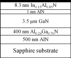 The new IEMN/RWTH/Aixtron HEMT InAlN/AlN/GaN heterostructure was grown using MOCVD on c-plane sapphire (Figure 1). This resulted in Hall mobility of ~1800cm2/V-s, sheet carrier density ~1.9x10¹³/cm2 and sheet resistance of 190Ω. “The very high electron mobility obtained on this epi-material indicates a very low interface roughness scattering at the hetero-interface and so a high crystal quality,” the researchers comment.
Figure 1: Schematic cross section of In0.15Al0.85N/AlN/GaN heterostructure on sapphire substrate.
The HEMTs were formed by first creating ohmic source/drain contacts of titanium-aluminum-nickel-gold that were annealed at 825°C for 30s in nitrogen. The devices were isolated with a helium ion implant. Measurements on two isolated ohmic contacts separated by 10μm gave a leakage at 200V for this isolation process of 10nA/mm. Transmission line model (TLM) structures gave an average contact resistance of ~0.6Ω-mm.
A ‘soft’ surface clean was performed using argon ion beam etching. A T-shape Schottky gate was formed of nickel-gold. The gate length/footprint was 225nm. A 240nm silicon nitride layer was used as passivation. The 2μm x 50μm wide gate was placed centrally in the space between the source and drain contacts, which were separated by 1.75μm.
The maximum drain current density at zero gate bias (VGS) was 1.22A/mm. Pinch-off occurred at –3.9V when the drain bias (VDS) was 6V. The maximum extrinsic peak transconductance reached 460mS/mm at VGS of –2.6V and VDS of 4V. The intrinsic maximum transconductance value of 692mS/mm under these bias conditions is derived from a source access resistance estimated at 7.2Ω, subtracting the effect of contact and sheet resistance.
The reverse gate leakage at –20V is 378μA/mm, which is considered to be a good value for an InAlN Schottky contact. Using a thermionic model, the Schottky barrier height is estimated at 1.11eV. Off-state breakdown at pinch-off occurred at 35V.
The radio frequency (RF) characteristics were obtained at drain and gate biases of 4V and –2.6V, respectively. The extrinsic current gain cutoff frequency (fT) was 52GHz and the maximum power gain cutoff frequency (fMAX) was 110GHz.
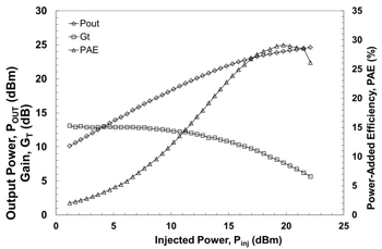 Figure 2: Output power, PAE and power gain versus injected power for InAlN/AlN/GaN HEMT at drain bias of 15V and gate bias of –3V.
Power measurements were carried out at 18GHz in class AB operation. The output impedance was adjusted to give maximum power density at each bias point. The maximum output power density of 2.4W/mm was achieved at a drain bias of 10V and a gate bias of –3V. Power-added efficiency (PAE) was 34% with 6dB compression level (a measure of non-linearity). At the higher drain bias of 15V (Figure 2) the power density was 2.9W/mm, but the power-added efficiency reduced to 26% with 6.5dB compression and linear power gain of 13.1dB.
The researchers propose that further surface pre-treatment and passivation optimization will lead to trap mitigation and increased device performance. Also, they believe that these devices could eventually beat the performance of more mature AlGaN/GaN HEMT technology, mainly through improving the ohmic performance of the source/drain contacts.
Back-barrier boosts nitride HEMT cut-off frequency
Quaternary nitride HEMT with record cut-off frequency
InAlN/GaN HEMTs Sapphire substrates MOCVD