- News
20 May 2011
Wafer bonding to be driven by small size wafers for LEDs and 12” wafers for 3D stacking & CIS
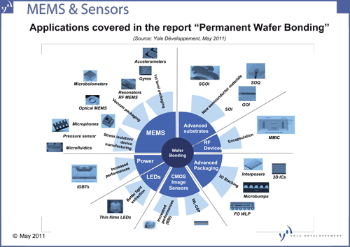
Historically developed for micro-electro-mechanical system (MEMS) and then silicon-on-insulator (SOI) substrates, wafer bonding technology is becoming a key processing technology for a wide range of applications, including CMOS image sensors (CIS), LEDs, power devices, RF devices and advanced packaging, according to market research firm Yole Développement in its ‘Permanent wafer bonding report’, which aims to give an overview across wafer bonding technologies over the 2010–2016 time frame.
The wafer bonding market is a very complex one spanning not only different applications but also different wafer sizes (from 2’’ to 12’’) and different bonding technologies (adhesive, anodic, fusion, direct oxide, eutectic, glass frit, metal diffusion).
Wafer bonding is usually defined as a process that temporarily or permanently joins two wafers or substrates using a suitable process. The technology has shifted to non-mainstream IC applications over the last years.
“MEMS has been the first application where wafer bonders have been massively used (the wafer bonding step is mostly used to protect the MEMS sensitive element),” says project manager Dr Eric Mounier. “CMOS Image Sensors is also a very promising application for wafer bonders,” he adds. Indeed, up to two different wafer bonding steps can be necessary for next-generation CMOS image sensors: one for back-side illumination and the second for wafer-level chip-scale packaging (WLCSP).
But besides MEMS and CIS, wafer bonder can be also used for LEDs and power devices. Indeed, in a typical LED active regions, spontaneous emission scatters photons in all directions. If the substrate material has a smaller band gap than the active region, about half of the light is absorbed in the substrate, significantly reducing device performance. So, one of the manufacturing solutions for photon loss involves bonding a wafer containing an array of devices to another wafer that provides both a reflective surface for maximum light extraction and a heat sink for thermal management. Also, of course, over the five past years much attention has been given to this technology for 3D integration of memories, for example.
For MEMS, there is currently a shift from glass frit for eutectic/metal-based bonding mainly to increase real estate through smaller bond frames. Metal direct bonding also gives good hermeticity and mechanical stability for many MEMS applications. For example, the Nasiri fabrication process uses eutectic bonding of the MEMS directly on the aluminium layer of the CMOS wafer. This leads to smaller package footprints and package heights. STMicroelectronics’ latest three-axis accelerometer (LIS3DH) also shows a different sealing technique compared to what is usually used: gold eutectic sealing allows a dramatic die size reduction.
For CMOS image sensors, the advent of back-side illumination technology has raised the competition between molecular bonding and adhesive bonding. Here, cost and the final application will drive the final choice of technology.
Yole forecasts rapid market growth for wafer bonding over the next year. Growth will be driven by small size wafers for LEDs and 12” wafers for 3D stacking and CIS.
Although EV Group is the market leader in permanent bonding, growth of the bonding equipment market is attracting challengers, notes Yole.
Companies cited in the report include: Acreo, AML, APM/UMC, Avago, Ayumi, Bosch, Colibrys, Dalsa, Discera, EV Group, FhG IMS, FLIR, IBM, Icemos, IMEC, IMT, Infineon, Infineon, Invensense, KTH, Leti, Lumileds, MEMStech, Micralyne, Mitsubishi Heavy Industries, Okmetic, Omron, Osram, Qualcomm, Raytheon, RPI, Sand9, Semefab, Sensonor, Silex, SOITEC, STM, SUSS MicroTEC, Tezzaron, TI, tMt, Tohoku University, TowerJazz, Tracit, Triquint, Tronic's, TSMC, VTI, Xcom, and Ziptronix.