- News
13 May 2011
VCSEL achieves 92W output record
Researchers in China have produced vertical-cavity surface-emitting lasers (VCSEL) with maximum peak output power of 92W obtained in pulsed operation at 110A, giving a power density of 15kW/cm2 [Lisen Zhang et al, Appl. Phys. Express, vol4, p052102, 2011].
The researchers, from Key Laboratory of Excited State Processes at Changchun’s Institute of Optics and Graduate School of the Chinese Academy of Science in Beijing, comment: “To the best of our knowledge, this is the highest value reported for a single device.” The room-temperature power output was limited by the capabilities of the power supply used.
VCSELs have many attractions such as low threshold currents, circular beams, high packing density in two-dimensional arrays, and single-mode emission. Solid-state laser devices tend to achieve higher output powers in pulsed operation. Such high output power can be applied to cutting, drilling and welding for medical and industrial applications. VCSELs have another advantage here, since they do not suffer from the catastrophic optical damage (COD) that afflicts the end facets of edge-emitting lasers at high field intensity.
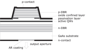 The main epitaxial structures of the Chinese device (Figure 1) were n- and p-type distributed Bragg reflectors (DBRs) sandwiching the active layer. These layers were grown using metal-organic chemical vapor deposition (MOCVD) on gallium arsenide (GaAs) substrates.
Figure 1: Schematic diagram of device structure.
The active region consisted of three quantum wells consisting of In0.2Ga0.8As in GaAs barriers. The wells had an emission wavelength around 980nm.
The n- and p-type DBRs were silicon and carbon doped, respectively. The DBRs were constructed from Al0.9Ga0.1As/GaAs pairs. The p-DBR consisted of 30 periods of quarter-wavelength thick layers giving 99.9% reflectivity. The n-DBR had 20 pairs of quarter-wavelength layers with 99.3% reflectivity. The interfaces between the layers were graded to reduce the series resistance of the DBRs.
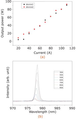 Figure 2. (a) Dependence of output power on injection current and (b) wavelength spectra at different injection currents under pulsed operation.
The reflectivity values of the DBRs were optimized, “balancing the threshold current and the output power to realize high differential quantum efficiency under pulsed operation.”
The device mesa was formed using a wet chemical etch. The selective oxide confinement was created by heating to 420°C in a humid atmosphere. The p-contact consisted of titanium-platinum-gold.
The laser beam was designed to emerge from the n-contact side — in other words, through the GaAs substrate. To enable this, hafnium dioxide (HfO2) was deposited on the substrate surface as an anti-reflective coat. The n-contact consisted of gold-germanium-nickel, which was evaporated around the HfO2 window. The aperture of the device was 500μm.
The device wafer was finally heated again in a rapid thermal anneal and then singulated. The singulated devices were soldered with indium junction-down on copper heatsinks.
The resulting laser diode suffered from self-heating effects. For example, in continuous-wave (CW) operation the slope efficiency was around 0.4W/A in the range 1–4A, and declined beyond that. Quasi-continuous operation (QCW, 50μsec pulse, 100Hz repetition) — to reduce thermal effects — increased this efficiency to about 0.6W/A over the range 1–6A. With pulsed operation (60ns pulse, 100Hz repetition), the efficiency increased up to 0.8–0.9W/A at 70A.
Another thermal effect is a red-shift in the emission wavelength (Table 1). From the observed red-shifts, the junction temperature rise in CW and QCW operation were estimated at 90°C and 20°C, respectively.
Operation |
Threshold |
Differential |
Maximum output |
Density |
Red-shift |
A |
Ω |
W |
W/cm2 |
nm/A |
|
CW |
0.8 |
0.8 |
1.62 @ 4.5A |
1.4 |
|
QCW |
0.8 |
0.12 |
2.89 @ 6A |
0.3 |
|
pulsed |
92 @ 110A |
15 |
0.0145 |
Table 1 (above).
Some of the same researchers produced a device with CW output power of 1.95W (0.93kW/cm2) in 2007. Princeton Optics reported a record 3W CW from a 350μm VCSEL in 2005.
VCSELs InGaAs GaAs substrates MOCVD
The author Mike Cooke is a freelance technology journalist who has worked in the semiconductor and advanced technology sectors since 1997.