- News
9 May 2011
Stepping up EBL in laser diode internal quantum efficiency
Researchers at Georgia Institute of Technology (GaTech) have used a stepped electron-blocking layer design for indium gallium nitride (InGaN) semiconductor laser diodes (LDs) to increase internal quantum efficiency (IQE) to 0.92, compared with 0.6 found for an unstepped layer [Yun Zhang et al, J. Appl. Phys., vol109, p083115, 2011]. The effects of the improvement in IQE were reduced threshold current densities for lasing (from 4.6kA/cm2 down to 2.5kA/cm2) and increased slope efficiency (from 0.72W/A up to 1.03W/A).
The researchers comment: “This simple yet efficient structural design change provides an effective way to achieve high-performance InGaN-based LDs with higher optical-output power and lower electric-power consumption.”
Electron-blocking layers (EBLs) are used to confine the electron and hole carriers to the active region of light-emitting devices in the hope of increasing internal quantum efficiency. In nitride semiconductor devices, the EBL often consists of a layer of aluminum gallium nitride (AlGaN), which has a wider bandgap than gallium nitride (GaN).
The EBL is deposited on the last barrier of the multi-quantum well (MQW) of the light-emitting device. The interface between the EBL and last barrier is usually strained, giving rise to polarization electric fields that are unusually strong in nitride semiconductors. These polarization fields lead to free-electron accumulation at the interface that degrades internal quantum efficiency of light emission.
To combat this effect, GaTech researchers produced two LD structures that differ in the EBL region: structure A had a conventional magnesium-doped p-Al0.16Ga0.84N layer on top of the last undoped 8.8nm GaN barrier of the active region; structure B also had a magnesium-doped p- Al0.16Ga0.84N, but the GaN barrier was replaced by two 4.4nm layers of p-AlGaN with stepped Al-content (Figure 1). The full epitaxial structures were grown using metal-organic chemical vapor deposition (MOCVD) on c-plane free-standing GaN substrates.
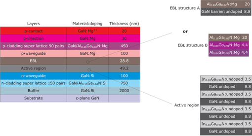
Figure 1: Compositions and thicknesses of LD structures.
LDs using epitaxial materials A and B were fabricated in the same process run to avoid fabrication-related performance variation. Ridge devices were formed with end facets that had distributed-Bragg-reflector (DBR) mirrors with reflectivities of 27% and 99%.
Optical output power-current density measurements on devices with 8μm x 750μm ridges in pulsed operation (0.1% duty cycle, pulse width 1μsec, repetition rate 1kHz), avoiding self heating effects, gave threshold current densities of 4.6kA/cm2 and 2.5kA/cm2 for structures A and B, respectively. The slope efficiencies were 0.72W/A for structure A, and 1.03W/A for structure B. The researchers also report that continuous-wave (cw) laser operation was achieved at room temperature for both structures.
By comparing devices with different cavity lengths, the researchers found the IQE and internal loss for devices based on epitaxial materials A and B. The IQEs were 0.6 and 0.92 for structures A and B, respectively. The loss values were roughly similar at 10/cm for structure A and 9/cm for structure B.
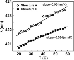 Spectral investigations showed variation of the peak wavelength with a red-shift at high temperatures (Figure 2). The staircase pattern for the peak wavelength of structure A is attributed to mode-hopping, where the stimulated emission switches from one longitudinal mode of the cavity to another as the temperature varies. Structure B has a smoother curve without mode hopping. The researchers comment: “The results suggest that the step-graded EBL design may offer a better thermal stability in the lasing wavelength.” Mode hopping in structure B was also suppressed at high injection current (and thus for high optical-output power operation).
Figure 2 (above right): Temperature dependence of peak wavelength for the LD structures A and B under pulsed-current operation from 20°C to 58°C.
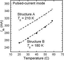 The shift in threshold current with temperature was also measured (Figure 3) to find the characteristic temperatures (T0) of the devices. The researchers comment: “It is noted that T0 of 210K on the abrupt EBL LDs is one of the highest values reported on InGaN-based violet-blue LDs. For the step-graded EBL LDs, T0 of 180K is also measured, which is comparable to typical values reported on other InGaN-based violet-blue LDs (140K-190K)”. A high value of T0 indicates less shift in the threshold with a given change in temperature.
Figure 3: Temperature dependence of the threshold currents for structures A and B in the pulsed-current mode from 20°C to 58°C.
The research at GaTech benefited from DARPA Visible InGaN Injection Lasers (VIGIL) program funding.
The author Mike Cooke is a freelance technology journalist who has worked in the semiconductor and advanced technology sectors since 1997.