- News
2 May 2011
ETH solves InP/GaAsSb maximum oscillation bipolar disorder
ETH-Zürich’s Millimeter-Wave Electronics Group has produced indium phosphide/gallium arsenide antimonide (InP/GaAsSb) dual-heterostructure bipolar transistors (DHBTs) with a maximum oscillation frequency (fMAX) exceeding 500GHz [Rickard Lövblom et al, IEEE Electron Device Letters, Vol. 32, No. 5 (MAY 2011), p629; published online 15 April 2011].
Traditional high-performance DHBTs use an indium phosphide/gallium indium arsenide (InP/GaInAs) structure. A potential advantage for using p+-GaAsSb for the base region is that a binary InP collector can be used due to the staggered band alignment between the materials, improving thermal conductivity and breakdown voltages of the structure – features that are desirable in high-efficiency power amplifiers. Unfortunately, GaAsSb-base DHBTs tend to have a low maximum oscillation frequency (fMAX) compared with the peak device cut-off frequency (fT).
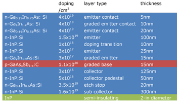 Figure 1: Epitaxial schematic of DHBT structure. Graded base has x varying between 0.42 (collector side) and 0.60 (emitter side). Graded emitter has y varying between 0.24 (base side) and 0.00 (emitter surface). Graded emitter contact has z varying between 0.49 and 0.25.
The epitaxial layers (Figure 1) were deposited on 2-inch indium phosphide substrates using metal-organic chemical vapor deposition (MOCVD). The double-heterostructure bipolar transistor was created using a triple mesa process to access the layers with contacts for the emitter, base and collector. The mesas for the emitter, base and collector were defined using electron-beam lithography, along with various wet and dry etch processes. The base–emitter junction was ~0.3μm wide. Several features of the transistor design, such as undercutting the base mesa under the metal, were designed to reduce capacitance in efforts to increase fMAX with respect to fT.
The researchers comment: “The present transistors are the first InP/GaAsSb DHBTs to feature fMAX> 500GHz, according to three extraction schemes”. These schemes were based on using Mason’s unilateral gain, single-pole fits, and ~20dB/dec extrapolations.
The fT cut-off was at 365GHz, while the peak current gain was 35. The sheet resistance of the base region of the transistor was 1160Ω/square. The common-emitter breakdown voltage (BVCEO) was more than 5.1V (open base) at a collector current density of 1kA/cm2.
The researchers believe that their device can be improved on by reducing the collector doping tail, creating a fully, rather than partially, depleted collector. The only partial depletion of the collector creates a higher capacitance between the base and collector, increasing signal delay times and slowing the device response.
The transistor process design aimed to reduce both the resistance of the base region (RB) and the capacitance between the base and collector (CBC), which are both factors that increase fMAX relative to fT (Equation 1). Although increasing the collector thickness (TC) reduces the base–collector capacitance, the researchers stress that this is not the only component of their fMAX improvement. To make their point, they compare their results (Table 1) with those of others using a figure of merit that eliminates the effect of the collector thickness (Equation 2).
![]()
Equation 1: Relation between fMAX, fT, RB and CBC.
fMAX |
fT |
TC |
F |
|||
GHz |
GHz |
nm |
GHz/nm |
|||
ETH |
2011 |
GaAsSb |
501 |
365 |
125 |
5.50 |
UIUC |
2008 |
GaAsSb |
420 |
480 |
100 |
3.68 |
Agilent |
2005 |
GaAsSb |
410 |
210 |
230 |
3.48 |
UCSB |
2011 |
GaInAs |
800 |
430 |
100 |
14.90 |
POSTECH/IntelliEPI |
2004 |
GaInAs |
687 |
215 |
250 |
8.78 |
UCSB/IQE |
2006 |
GaInAs |
218 |
660 |
60 |
1.20 |
Table 1: Comparison of ETH transistor with similar devices produced by others (University of Illinois at Urbana-Champaign, UIUC; Agilent Techologies, Agilent; University California Santa Barbara, UCSB; Pohang University of Science and Technology/Intelligent Epitaxy Technology, POSTECH/IntelliEPI; University California Santa Barbara/IQE, UCSB/IQE) using both GaAsSb and GaInAs base regions.
![]()
Equation 2: Equation for figure of merit (F) used by ETH.
The researchers comment on the wide spread for F in the InP/InGaAs devices: “The wide range of Fs for GaInAs HBTs suggests caution in drawing comparisons across different materials and process technologies: F is probably most helpful to track the evolution of a given technology”.
http://dx.doi.org/10.1109/LED.2011.2118738
The author Mike Cooke is a freelance technology journalist who has worked in the semiconductor and advanced technology sectors since 1997.