- News
29 March 2011
Simulating way to improved DUV LEDs
Researchers at Taiwan National Changhua University of Education and LED chip maker Epistar Corp have carried out simulations that suggest that deep-ultraviolet (DUV) light-emitting diodes (LEDs) could benefit from using multi-quantum well (MQWs) structures with barrier thicknesses that vary through the structure [Miao-Chan Tsai et al, Appl. Phys. Lett., vol98, p111114, 2011]. In particular, having thicker barrier layers towards the p-type end of the simulated device increased the light output power by 45% at 20mA injection current.
In the past few years, a number of research groups have reported deep-ultraviolet (less than 300nm wavelength) LEDs, based on the aluminum gallium nitride (AlGaN) semiconductor material system. The output powers are generally low (less than 1mW or even 1μW at wavelengths less than 250nm) and there is much interest in increasing the efficiency of devices.
The main application in the short term would be the replacement of mercury lamps, which are inefficient, unreliable, short-lived and environmentally undesirable (particularly in terms of disposal). The first application in line for conversion to these devices is thought to be disinfection lamps, since UV light of these wavelengths disrupts biological structures, killing microbes etc. Further possible applications include gas sensing, medicine, and biochemical analysis.
As a basis for their work, the Taiwan researchers used a previously published actual device structure (Figure 1) developed by Japan’s Institute of Physical and Chemical Research (RIKEN) and Saitama Univensity [Hideki Hirayama et al, Appl. Phys. Lett., vol91, p071901, 2007, http://link.aip.org/link/doi/10.1063/1.2770662]. These devices were 300μm square and emitted 261nm-wavelength radiation.
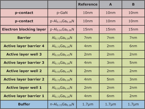
Figure 1: Basic device structure with triple quantum well active region from Japanese research, and the graded barrier structures modeled by the Taiwan team.
The Taiwan research group has previously found that decreasing the barrier thicknesses towards the p-contact end of a multi-quantum well (MQW) active layer improved hole injection for a blue-emitting indium gallium nitride LED structure in simulation. Sufficient hole injection is a challenge for all nitride semiconductor light-emitting devices due to the high activation of magnesium (Mg) doping (reducing hole carrier densities in p-type materials).
For deep-UV emission (less than 300nm), the Taiwan researchers produced simulations of variations of the RIKEN/Saitama LED, varying the barrier thicknesses from 6nm to 2nm. ‘Structure A’ decreased the barriers from n-type to the p-type region, while ‘structure B’ increased the barrier thickness in the same direction (Figure 1). The work was also checked by a reference simulation with constant 4nm barriers, as in the RIKEN/Saitama device.
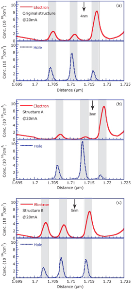 Figure 2: Electron and hole concentrations of (a) original structure, (b) structure A, and (c) structure B around the active region at 20mA. Note that the scale of the hole concentration axis is two orders of magnitude smaller than that for the electrons.
The simulations suggest that the hole concentration is very low (about two factors of ten down from the electron density) in the active layer for the three structures considered (Figure 2). This is due to the low hole concentration in the p-AlGaN layers, along with valence-band offsets between the p-type layers, making it difficult for holes from the p-GaN layer to reach into the light-emitting region. The p-GaN layer has a higher hole concentration due to the lower activation energy of the Mg doping. The electron-blocking layer (EBL) is also inefficient at completely blocking electrons from entering and recombining (generally non-radiatively) in the p-type regions.
The low hole density in the active layers means that there are a large number of electrons that do not recombine. Negative outcomes from this include serious electron leakage, more non-radiative recombination, self-heating problems, and poor output power.
The obvious solution might appear to be to thin the barrier towards the p-end of the device, allowing in more holes (structure A). However, the Taiwan simulations suggest that while the hole concentration in the middle well increases, it does not match up with the electron distribution, which is concentrated towards the p-end of the active region.
The counter-intuitive structure B leads to a more balanced hole (and electron) distribution. The researchers attribute this to a smaller electrostatic field and smoother energy-band profile in the thicker barrier at the p-end.
Further simulation work consisted in determining the amount of non-radiative electron–hole recombination (Shockley–Read–Hall mechanism). They found that the radiative recombination in structure A was 50% that of the reference device, while structure B radiation rates were increased 56%.
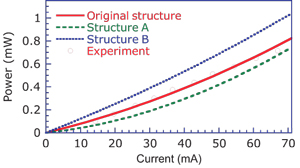 Figure 3: Output power as a function of current for the original structure, structure A, and structure B. The open circles are the experimental data of the original structure produced by Japanese researchers.
Bringing all the work together, the researchers calculated light output versus current for the three structures and compared their results with the Japanese experiments to demonstrate the reliability of the simulations (Figure 3). At 20mA, the structure B emitted 45% more power than the reference device.
The researchers used Crosslight Software’s APSYS, Advanced Physical Models of Semiconductor Devices, simulator.
Liquid phase pushes deep ultraviolet to higher efficiency
Lateral conduction, substrate-free deep UV nitride semiconductor LEDs
http://link.aip.org/link/doi/10.1063/1.3567786
www.epistar.com.tw/index_en.php
The author Mike Cooke is a freelance technology journalist who has worked in the semiconductor and advanced technology sectors since 1997.
Join Semiconductor Today's LinkedIn networking and discussion group