- News
23 March 2011
Back-barrier to InAlN HEMT short-channel effects
Researchers at Massachusetts Institute of Technology (MIT) and IQE RF LLC in the USA have used an aluminum gallium nitride (AlGaN) back-barrier to improve the frequency performance of indium aluminum nitride (InAlN) high-electron-mobility transistors (HEMTs) [Dong Seup Lee et al, IEEE Electron Device Letters, published online 3 March 2011].
The MIT/IQE researchers say that their work is the first use of AlGaN as a back-barrier in an InAlN/GaN device. The aim of the back-barrier is to maintain the performance of smaller (‘scaled’) devices. In particular, the researchers wanted to reduce ‘short-channel effects’ such as drain-induced barrier lowering (DIBL). These effects arise due to the reduced charge density in the two-dimensional electron gas (2DEG) channel and increased gate leakage current arising from the use of thinner barrier layers. With an AlGaN back-barrier, it is hoped to maintain performance with thicker InAlN top-barriers.
Unlike the AlGaN alternative, InAlN layers can be grown lattice matched to GaN if an In fraction of 17% is used. Also, with In0.17Al0.83N there is a large polarization discontinuity with GaN, leading to higher charge densities in, and larger band offset to, the GaN channel, compared with AlGaN/GaN. These features allow sheet resistances for InAlN/GaN structures to be less than 300Ω/square.
The barrier thickness of the InAlN in HEMT devices also tends to be thinner (less than 10nm) than with the corresponding AlGaN HEMTs. A thinner barrier layer removes the need to etch the top-barrier to bring the gate electrode closer to the channel (recessed gate), as is commonly done in making smaller AlGaN HEMTs. Avoiding etch processes is desirable in terms of reducing plasma damage of the device, which can adversely affect performance.
 These features have enabled InAlN devices with current densities up to 2.5A/mm and cut-off frequencies (fT) up to 245GHz. A further feature of nitride semiconductor devices is the potential for operation in harsh environments. On this line, one group has reported InAlN/GaN HEMT operation at temperatures up to 1000°C.
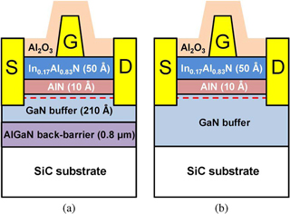
Figure 1: Schematics of InAlN/GaN HEMTs with and without an AlGaN back barrier.
The MIT/IQE HEMT structures (Figure 1) were grown on silicon carbide (SiC) substrates using metal-organic chemical vapor deposition (MOCVD). The further processing of the epitaxial material into transistor structures (mesa isolation etch and metal contact deposition/anneal) was carried out at the same time with the standard and back-barrier HEMTs. The ohmic source–drain contacts consisted of titanium-aluminum-nickel-gold and the Schottky gate consisted of nickel-gold. A final aluminum oxide layer was (deposited by atomic-layer deposition) acts as passivation.
Although the epitaxial material with back-barrier has a higher mobility (1635cm2/V-s vs 1369cm2/V-s without), the carrier density is lower (1.1x10¹³/cm2 vs 1.7x10¹³/cm2) and the sheet resistance higher (310Ω/sq vs 260Ω/sq). These factors lead to reduced maximum drain current (1.49A/mm vs 2.05A/mm at 2V gate potential) and higher threshold voltage in DC operation for 65nm gate-length devices. Higher access resistance reduces the extrinsic transconductance (gm) to 539mS/mm, which is 9% lower than the standard device without back-barrier (592mS/mm).
At high biases, the back-barrier device also suffers from self-heating effects such as low saturation current. This is caused by the relatively low thermal conductivity of the AlGaN back-barrier material.
One good DC feature of the back-barrier device is smaller drain-induced barrier lowering (DIBL) at shorter gate lengths due to the smaller output conductance. Above a gate length of 100nm, the DIBL values of both devices are less than 50mV/V. Below 100nm, the DIBL of devices without back-barrier increases sharply, while that of back-barrier HEMTs remains in the 50–60mV/V range.
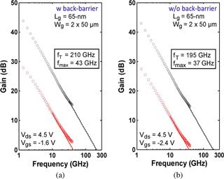 Figure 2: RF performance of 65nm-gate-length InAlN/GaN HEMTs (a) with and (b) without AlGaN back barrier.
Operation at microwave frequencies from 450MHz up to 40GHz was also tested (Figure 2). The maximum cut-off frequency (fT) conditions were a drain bias of 4.5V and a gate potential of –1.6V for the back-barrier HEMT, and 4.5V and –2.4V, respectively, for the standard device without back barrier. The measured maximum fTs were 210GHz and 195GHz for the back-barrier and standard HEMTs, respectively. The researchers attribute this 8% gain in fT as being due to the high output resistance of the back-barrier HEMT.
“It is expected that the improvement becomes even more important as the gate length scales below 50nm,” the researchers comment.
The maximum oscillation frequency (fmax) was relatively small in both devices due to high resistance of the thin rectangular gate.
Financial support for the research came from the US Defense Advanced Research Projects Agency NEXT, a National Science Foundation CAREER Award, and the Office of Naval Research DURIP program.
InAlN HEMT InAlN/GaN MOCVD SiC substrates IQE
The author Mike Cooke is a freelance technology journalist who has worked in the semiconductor and advanced technology sectors since 1997.
Join Semiconductor Today's LinkedIn networking and discussion group