- News
7 March 2011
Self-organized process for light boost
Researchers in the USA and South Korea have used a ‘self-organized’ silver mask to create nanotexturing and to boost the light output by 46% from a nitride semiconductor light-emitting diode (LED) at 100mA, compared with a device that has a flat nitride–air interface [Sameer Chhajed et al, Appl. Phys. Lett., vol98, p071102, 2011]. The nanotexturing reduces light reflection back into the device at the p-type gallium nitride (GaN) surface.
A planar GaN surface has a refractive index of 2.5, resulting in 18% normal incidence reflection at an air interface (refractive index 1). Also, the critical angle for total internal reflection is only 23°, severely restricting light output. In total, a planar GaN–air interface gives the LED an extraction efficiency of about 26%.
The USA’s Rensselaer Polytechnic Institute (RPI) and South Korea’s Pohang University of Science and Technology used oblique angle deposition of silver on the p-GaN surface to create nano-island masking for a short etch process that roughened the surface of the contact layer, improving light extraction. A self-organized process is attractive in terms of reduced complexity and higher throughput.
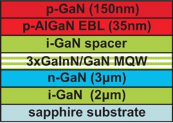 Gallium indium nitride (GaInN) LED epitaxial structures (Figure 1) were grown on sapphire substrates using metal-organic chemical vapor deposition (MOCVD). This epitaxial material was used to create ‘reference’ and ‘nanotextured’ LEDs (blue emission wavelength, 460nm) after annealing for 1 minute at 800°C to activate the p-GaN layer.
Figure 1: Epitaxial structure of GaInN-based LEDs used by RPI.
In both cases the epitaxial material had mesa structures defined using photolithography and etched down to the n-GaN layer using reactive-ion etch with inductively coupled plasma (ICP-RIE) generated from a chlorine and boron trichloride mix (Cl2/BCl3). The mesas were 1mm square. The n-type ohmic contact metal structure was titanium-aluminum-titanium-gold, deposited using electron-beam (e-beam) evaporation. The non-p-contact regions were then masked off using photolithography.
The nanotexturing (if any, Figure 2) occurred before application of the p-contact metal (10nm semi-transparent palladium). The mask for the nanotexture consisted of a 5nm silver layer deposited at a 60° oblique angle, again using e-beam evaporation. The effect of the oblique angle is to create ‘self-organized’ islands of silver on the surface of the p-contact (and, incidentally, the litho-mask). The p-contact surface was then exposed for 15 seconds to Cl2/BCl3 ICP-RIE. The silver mask was removed using a 70% nitric acid solution. The researchers comment that their method does not involve deposition of sacrificial layers or high-temperature annealing that could damage previous work.
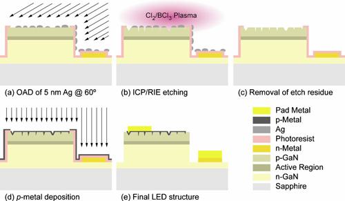
Figure 2 (above): Schematic fabrication process flow of nanotextured p-type GaN mesa of a GaInN LED.
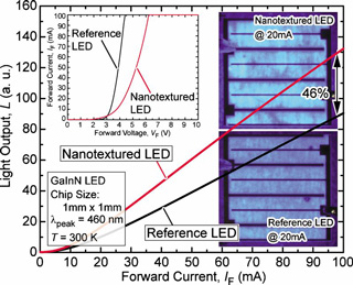 Figure 3 (right): Light-output power vs forward current plots of reference and nanotextured LEDs. Inset: forward current vs forward voltage characteristics of LEDs. Photographs of illuminated LEDs at 20mA are shown in background.
Analysis of the light output power of the two devices with pulsed drive current (1% duty cycle, pulse width 0.5 milliseconds) gives a 46% enhancement for the nanotextured LED over the reference at 100mA (Figure 3). The current–voltage dependence of the devices shows that the nanotextured LED has higher series resistance, attributed to contact resistance and current crowding effects. These effects are thought to result from the reduction of the effective contact area from the nanotexturing process. The researchers hope to mitigate the high resistance through future optimization work.
RPI’s contribution was supported financially by the US National Science Foundation (NSF), Samsung LED Co and New York State Energy Research and Development Authority (NYSERDA).
Blue LEDs GaInN GaN Sapphire substrates Nanotextured
The author Mike Cooke is a freelance technology journalist who has worked in the semiconductor and advanced technology sectors since 1997.
Join Semiconductor Today's LinkedIn networking and discussion group