- News
9 March 2011
Liquid phase pushes deep ultraviolet to higher efficiency
Boston University has produced deep ultraviolet light-emitting diodes from epitaxial nitride semiconductor material that demonstrates a high internal quantum efficiency (IQE) of 32% under photoluminescence (at 300nm wavelength) at room temperature [Yitao Liao et al, Appl. Phys. Lett., vol98, p081110, 2011].
The Boston research group has previously developed aluminum gallium nitride (Al0.7Ga0.3N) epitaxial quantum well (QW) structures with AlN barriers that emitted at 220nm and 250nm with room-temperature IQEs of 5% and 50%, respectively [A. Bhattacharyya et al, Appl. Phys. Lett., vol94, p181907, 2009]. The difference between the two IQEs was explained as being due to the lower III/V ratio (~1) for the 220nm material growth, as opposed to the 250nm (>> 1, achieved through higher Ga flux), despite the fact that the compositions of the wells should have been the same (Al0.7Ga0.3N). At that time (May 2009), the researchers did not produce LEDs but, since high IQE has now been achieved at room temperature, device demonstrators become feasible.
The researchers believe that their plasma-assisted molecular beam epitaxy (PAMBE) growth with high Ga-flux converts the deposition process from being vapor phase epitaxy (VPE) to liquid phase epitaxy (LPE), with the Ga atoms forming a thin liquid layer on the surface of the growing crystal. The Boston group believes that one effect of LPE is to create AlGaN layers with lateral compositional inhomogeneities and thus deep band-structure potential fluctuations.
Professor Theodore D. Moustakas, leader of the Boston group, comments: “As a result, the injected electron–hole pairs form excitons localized in these potential fluctuations, which prevents them from migrating and recombining non-radiatively at point or line defects. Such phenomena occur automatically in indium gallium nitride (InGaN) QWs because of the tendency for phase separation due to the 11% difference in the size of In and Ga ions. On the other hand such phase separation is not expected in AlGaN since the Al and Ga atoms have near identical ionic radius.”
Moustakas adds: “A further advantage of our LPE growth mode is that it prevents the incorporation of oxygen, which is always present in the process gases as a major impurity, and introduces states in the middle of the gap in high-Al% AlGaN alloys. This is to be contrasted with InGaN alloys in which oxygen introduces shallow states which act as donors.”
According to Moustakas, MBE is also much simpler and potentially more economical than the traditional metal-organic chemical vapor deposition (MOCVD) process, which is traditionally used for the growth of this family of materials and devices.
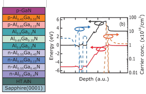 The active region of material used in the latest research consisted of a 3nm single quantum well between asymmetric barriers (Figure 1). The barrier on the n-side was 10nm and that on the p-side 5nm. The purpose of this was to balance the numbers of holes and electrons in the well, since holes find it harder than electrons to diffuse over barriers.
Figure 1: Schematic of the investigated deep UV LED structure (left), with thermal equilibrium band diagram and carrier densities of the structure (right).
A complex n-side sequence was designed to avoid nucleation and propagation of cracks through subsequent layers, and to improve electron injection into the well. The initial AlN layer was 2μm thick. The n-Al0.6Ga0.4N layer had a doping profile that increased in three steps from the mid 1017/cm3 range to a final layer that was doped to give a free-electron concentration of more than 1019/cm3, for a good n-contact. The polarization profile of the uniformly doped n-type AlGaN layer sequence with 55%, 85% and 55% Al was designed to boost electron injection. A similarly enhanced injection of holes was expected from inserting 45% Al-content p-AlGaN between the p-GaN contact and p-Al0.85Ga0.15N electron-blocking layer.
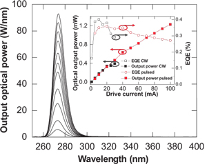 The epitaxial material was processed into 300μm square DUV LEDs using standard processes (lithography, etch). The chip was flip-chip bonded onto a silicon submount. The emission consisted of a single peak at 273nm (Figure 2). The full-width at half-maximum (FWHM) was 9nm. Under continuous-wave (cw) operation, optical output power saturated at 0.38mW with 25mA drive current, due to self-heating effects. Pulsed operation allowed the output power to increase to 1.3mW at 100mA. The maximum external quantum efficiency was 0.4%.
Figure 2: Electroluminescence (EL) spectra of 273nm UV LED measured under pulsed mode. Inset: integrated output power and the EQE under cw and pulsed injection.
Moustakas draws the conclusion from his group’s work that AlGaN QWs can be made to have the same IQE as that of InGaN QWs and that therefore the poor external quantum efficiency (EQE) of current-generation LEDs is the result of poor injection and/or extraction efficiencies.
Some of the funding for the work was derived through a Boston University–US Army Research Laboratory (ARL) research co-operation agreement.
Lateral conduction, substrate-free deep UV nitride semiconductor LEDs
http://link.aip.org/link/doi/10.1063/1.3559842
The author Mike Cooke is a freelance technology journalist who has worked in the semiconductor and advanced technology sectors since 1997.
Join Semiconductor Today's LinkedIn networking and discussion group