- News
13 June 2011
Nitride HEMTs grown on CMOS-compatible silicon
Researchers based in Switzerland and France have produced aluminum gallium nitride (AlGaN) barrier high-electron-mobility transistors (HEMTs) on high-resistivity silicon (Si) substrates oriented in a direction compatible with mainstream complementary metal-oxide-semiconductor (CMOS) integrated circuits [Diego Marti et al, Appl. Phys. Express, vol4, p064105, 2011]
The work was carried out at ETH-Zürich’s Millimeter-Wave Electronics Group and Centre de Recherche sur l’Hétéro-Epitaxie et ses Applications of France’s Centre National de la Recherche Scientifique (CRHEA-CNRS). The researchers comment on their achievement: “DC and RF performance of short-gate-transistor AlGaN/GaN HEMTs grown on (110) high-resistivity (HR) Si is reported for the first time.”
Nitride HEMTs are being intensively developed for power amplification of radio-frequency signals and for high-power switching. The possibility of manufacture on silicon substrates promises lower production costs and hence wider application of such devices.
Previous nitride HEMTs on silicon substrates have used wafers that are oriented in the (111) crystal direction since they present a hexagonal surface that is better suited to growing wurtzite epilayers such as GaN. However, Si(111) material has poor properties in terms of CMOS circuit elements. Researchers (and manufacturers) would like to develop integrated circuits that combine the advantages of nitride HEMTs and silicon CMOS.
While the Si(001) crystal orientation is preferred at the moment in mainstream CMOS, it is difficult to grow high-quality crack-free nitride material on such wafers, limiting HEMT cut-off (fT) and maximum oscillation (fMAX) frequencies to less than 37GHz and 55GHz, so far.
Another possible silicon orientation is (110), which has even been proposed as a booster of conventional CMOS due to improved channel transport in ultra-thin-body silicon-on-insulator CMOS devices. Nitride semiconductor devices (blue light-emitting diodes, long-gate transistors, etc) grown on Si(110) have shown similar characteristic to those grown on Si(111) substrates.
Now, having produced the first AlGaN/GaN HEMTs on Si(110), the ETH/CNRS researchers conclude: “The results indicate that is possible to fabricate GaN HEMTs on a Si(110) substrate, suggesting that GaN epitaxy on (110) Si provides a promising avenue for the future integration of GaN and mainstream CMOS technology on a (110) Si platform.”
The researchers used molecular beam epitaxy (MBE) to grow the HEMT epilayers on 2-inch high-resistivity Si(110) substrates. The Si wafer surface was prepared by etching away the native oxide layer with hydrofluoric acid and rinsing in deionized water before the MBE processing.
Nucleation (43nm AlN at 920°C) and stress-mitigating (250nm Al0.15Ga0.85N, 800°C; 250nm AlN, 920°C) layers were applied before the 1.7μm GaN buffer. The active layers consisted of 1nm AlN spacer, 18nm undoped Al0.29Ga0.71N barrier, and 3nm GaN cap. The purpose of the spacer was to reduce alloy scattering in the two-dimensional electron gas (2DEG) that forms at the GaN buffer-AlGaN barrier interface to provide the channel in HEMTs.
The resulting structure was subjected to a number of standard structural and electrical tests (Table 1). According to the researchers, the GaN (302) x-ray diffraction peak result is directly connected to the density of threading dislocations and, on the basis of their previous research, is assigned a value of not more than 4x10⁹/cm2.
Substrate |
Si(110) |
GaN thickness |
1.7μm |
X-ray diffraction (002) peak full-width half-maximum |
1044arcsec |
X-ray diffraction (302) peak full-width half-maximum |
1764arcsec |
Substrate bow |
50μm |
Carrier sheet density from capacitance-voltage measurements |
1x10¹³/cm2 |
Pinch-off voltage |
-5.3V |
GaN background doping, n |
1x10¹⁴/cm3 |
Carrier sheet density from Hall measurements |
9.70x10¹²/cm2 |
Mobility from Hall measurements |
2047cm2/V-s |
Table 1: Structural and electrical properties of the AlGaN/GaN heterostructure grown on Si(110).
HEMTs were created with titanium-aluminum-molybdenum-gold ohmic contacts and nickel-platinum-gold Schottky metal gate electrodes. Devices with varying gate lengths of 50nm, 75nm and 100nm were produced. The head height and stem width of the gates were 120nm and 400nm, respectively. The devices were isolated on etched mesas. Silicon nitride was used as a passivation layer. The contact pads consisted of titanium-gold.
The DC performance was similar for all three gate lengths with maximum drain current of 1.2A/mm for zero gate potential. The maximum transconductance of 250mS/mm occurred at –4.5V gate potential and 6V drain bias. At –7V gate potential, the gate leakage was 7.5μA/mm.
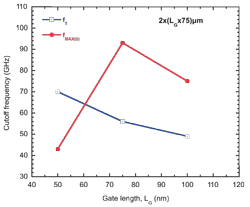 The raw cut-off (fT) and maximum oscillation (fMAX) frequencies, without de-embedding the contacts, were 44GHz and 39GHz, respectively. On-wafer calibration structures were used to de-embed the effect of the contacts on frequency performance through appropriate extrapolations. The maximum fT of 70GHz was obtained for the 50nm short-gate device, while the best fMAX was demonstrated by the intermediate 75nm gate (Figure 1). The researchers explain this as being due to a trade-off between increased gate resistance as the gate length shortens and a decrease in fT as the gate covers more area.
Figure 1: Dependence of fT and fMAX on gate length (LG).
UCSB reports N-polar HEMT power density record
The author Mike Cooke is a freelance technology journalist who has worked in the semiconductor and advanced technology sectors since 1997.