- News
16 June 2011
Record transconductance for nitride HEMT on silicon
Institut d'Electronique, de Microélectronique et de Nanotechnologie of France’s Centre national de la recherche scientifique (IEMN/CNRS) has produced nitride semiconductor high-electron-mobility transistors (HEMTs) on silicon with record transconductance of 470mS/mm [F. Medjdoub et al, Appl. Phys. Lett., vol98, p223502, 2011].
The team used an ultra-thin aluminium nitride (AlN) barrier on gallium nitride (GaN) buffer to achieve this performance, building on their recent achievement of 2A/mm output current with a similar device [AlN barrier increases output current from GaN/Si HEMTs].
The epitaxial material used to create the new HEMTs was again supplied by IMEC spin-off EpiGaN, based in Belgium. The structure, grown on highly resistive Si(111) wafers using metal-organic chemical vapor deposition (MOCVD), was similar to the recent report from IEMN, except that the AlN barrier layer was halved in thickness to 3nm. The in-situ SiN layer prevents cracking of the surface, reduces roughness, and also acts as passivation of surface charges that can deplete the two-dimensional gas (2DEG) that forms in the barrier–buffer region, creating the channel conduction mechanism.
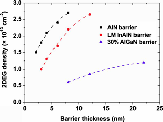 The use of AlN rather than AlGaN enables 2DEG carrier densities to be adequate even at 3nm for HEMTs. By contrast, the traditional AlGaN barrier 2DEG carrier density becomes less than 1013/cm2 for thicknesses less than 10nm (Figure 1). Although lattice-matched (LM) In0.17Al0.83N has much better performance in this respect than AlGaN, it is beaten by AlN.
Figure 1: Room-temperature 2DEG carrier density measured by Van Der Pauw method of SiN/AlN/GaN, lattice matched In0.17Al0.83N/GaN, and Al0.3Ga0.7N/GaN heterostructures as a function of the barrier layer thickness.
The ohmic contacts of the HEMT were formed by etching into the in-situ SiN, depositing titanium-aluminum-nickel-gold layers on the AlN barrier, and then annealing at 900°C in nitrogen. Helium implantation was used to isolate the devices.
The 0.2μm gate-length electrode was created by etching into the SiN with a sulfur hexafluoride plasma (SiN/AlN selectivity factor of 90), and then depositing nickel-gold layers. The devices were 50μm wide with gate–source and gate–drain distances of 0.4μm and 1.3μm, respectively.
An additional passivation layer of 200nm SiN was applied using plasma-enhance chemical vapor deposition (PECVD).
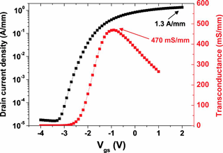 Although the output current density is reduced from the performance of the previous device (1.3A/mm rather than 2A/mm, both at +2V gate potential), the new device has a peak extrinsic transconductance “beyond the highest value of any GaN-based HEMT structure grown on Si substrate”. The new device with ultra-thin 3nm AlN barrier has a transconductance of 470mS/mm (Figure 2), compared with 390mS/mm for the previous device with 6nm AlN, both results measured at 10V drain bias.
Figure 2: Transfer characteristics of the 0.2μm x 50μm SiN/AlN/GaN HEMT on silicon substrate, demonstrating a record extrinsic transconductance of GaN-on-Si HEMTs.
The researchers attribute the enhanced transconductance to high 2DEG density and a short gate-to-channel distance. The gate and drain leakage currents are estimated to be less than 20μA/mm.
The team concludes: “These results show that this highly scalable technology should offer unprecedented frequency operation considering the high aspect ratio achievable with sub-100nm gate lengths and the great AlN/GaN-on-Si material quality already obtained. Therefore, breakthrough millimeter-wave performances can be expected in a cost-effective way using this heterostructure.”
The researchers also carried out capacitance–voltage and current–voltage measurements on circular 50μm-diameter diodes to investigate the carrier density profile and leakage characteristics of the epitaxial material. The high polarization between the 3nm AlN layer and GaN buffer was seen to provide sharp carrier confinement of the 2DEG at the interface. Low leakage (less than 10μA) was seen below 0V (i.e. reverse bias) down to –200V. This suggests there is no electron tunneling through the AlN barrier. The forward diode characteristic had an ideality factor of 1.35 with a potential barrier height of 1.2eV.
Nitride HEMTs grown on CMOS-compatible silicon
AlN barrier increases output current from GaN/Si HEMTs
The author Mike Cooke is a freelance technology journalist who has worked in the semiconductor and advanced technology sectors since 1997.