- News
2 June 2011
AlN barrier increases output current from GaN/Si HEMTs
Researchers based in France have developed high-electron-mobility transistors (HEMTs) using gallium nitride (GaN) on silicon substrates with output current densities exceeding 2A/mm [F. Medjdoub et al, IEEE Electron Device Letters, published online 16 May 2011]. The team from Institut d'Electronique, de Microélectronique et de Nanotechnologie of France’s Centre national de la recherche scientifique (IEMN/CNRS) comments that this “represents, to the best of our knowledge, the highest value ever achieved for GaN-on-Si HEMTs.”
The devices used ultra-thin aluminum nitride (AlN) barrier layers to maximize carrier densities in the channel, reducing on-resistance.
Nitride semiconductor material has a number of properties that make it an attractive base for microwave power electronics applications. Among these characteristics, the large polarization charge can be used to create two-dimensional electron gases (2DEGs) with high carrier density and hence low resistance. The wide bandgaps of nitride semiconductors also enable high power densities, and these materials’ high thermal conductivity can be used to dissipate the generated heat effectively.
In conventional HEMTs, an aluminum gallium nitride (AlGaN) barrier layer is deposited on a GaN buffer, creating a 2DEG at the interface. As the barrier layer becomes thinner, the charge density decreases. Unfortunately, thinner barrier layers are needed to access high-frequency performance.
A further disadvantage is that thinner barriers make it more difficult to isolate the gate electrode from the channel, requiring the use of gate dielectric insulation, rather than a simpler Schottky contact, to reduce gate leakage currents. The processes used to apply dielectrics or to bring the electrode closer to the channel (recessing) tend to degrade the reliability of devices.
High-aluminum-content barriers of indium aluminum nitride (InAlN) or even AlN, which has the highest spontaneous polarization of all the III–N materials, have lately been used to maximize 2DEG charge densities with promising results, suggesting useful performance up to W-band microwave frequencies (75–110GHz).
Another recent development in nitride semiconductors is their growth on large-diameter silicon substrates (up to 6 inch/150mm). This suggests the possibility of low-cost, large market adoption of nitride semiconductor electronics.
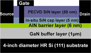 The epitaxial structures (Figure 1) used by IEMN/CNRS were grown on highly resistive (more than 5000Ω-cm) 4-inch Si(111) substrates. The epi-material was supplied by IMEC spin-off EpiGaN, based in Belgium. The ultra-thin barrier layer of 6nm is less than the critical thickness of 9nm above which the crystal quality of AlN epitaxial layers degrades, but is still subject to a high amount of tensile stress due to the lattice mismatch between AlN and GaN. A 5nm Si3N4 cap layer was grown in-situ on top of the AlN with the aim of handling this tensile stress and to give a high-quality surface.
Figure 1: Cross section of fabricated AlN/GaN-on-Si HEMTs.
Ohmic source drain contacts consisted of titanium-aluminum-titanium-gold, deposited on the AlN barrier material and annealed at 900°C in nitrogen, after etching through the SiN layer. Helium was implanted to isolate devices.
More silicon nitride was deposited using plasma-enhanced chemical vapor deposition (PECVD), before gate formation. The nickel-gold 0.2μm gate was deposited after photolithography and plasma etching through the SiN. The gate–source and gate–drain distances were 0.4μm and 1.3μm, respectively. The width of the device was 50μm. A further 200nm PECVD SiN layer was added as passivation.
The high output drain current density of up to 2.03A/mm is attributed to the high sheet electron carrier density (2.15x1013cm2) that results from using a barrier constructed from AlN.
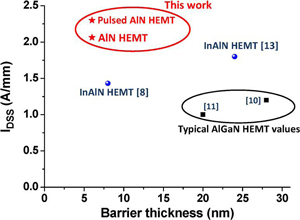 Figure 2: Benchmarking of saturated maximum output current density (IDSS) of GaN-on-Si HEMTs as function of barrier thickness for AlGaN/GaN (black squares), InAlN/GaN (blue circles), and AlN/GaN heterostructures (red stars).
Pulsed operation (500ns, 1% duty cycle) gave an even higher drain current, with densities up to 2.3A/mm. The difference in behavior was attributed to the limited thermal dissipation of the silicon substrate when the device is subjected to direct current. The researchers report slight gate and drain lag effects due, it is thought, to damage from the gate etch process that needs to be further optimized.
The breakdown voltage with the gate potential of –8V and a drain current of 1mA/mm is about 38V for a device with a gate–drain spacing of 1.3μm. Increasing the gate–drain spacing to 3μm increases the breakdown voltage to more than 100V.
The peak extrinsic transconductance is 390mS/mm, with a drain bias of 10V and a gate potential of –4V. The calculated intrinsic transconductance (i.e. removing the effect of access resistance) is as high as 600mS/mm. The researchers credit the short gate–channel distance for this.
Also, a low gate leakage of 20μA/mm is attributed to high AlN growth quality along with robustness of the surface enhanced by the in-situ SiN cap layer. The researchers comment: “It has to be noted that avoiding gate recess and gate insulator while achieving both high aspect ratio and low leakage current should be definitely advantageous to the device reliability”.
The frequency dependence of the device was measured between 10MHz and 50GHz to extract a current gain extrinsic cut-off (fT) frequency and a maximum oscillation (fMAX) frequency of 52GHz and 102GHz, respectively. The researchers see the high fMAX/fT ratio as a promising feature for good device performance. “Moreover, the fTxLg product of 10.4GHz-μm is favorably comparable to that of the reported state-of-the-art GaN-on-Si HEMTs using an 80nm gate length.” Very high-frequency operation could result from down-scaling the technology to sub-100nm gate lengths, the researchers believe.
The team concludes: “These results reflect the great AlN/GaN material quality already obtained and the maturity of the processing technology, which promise breakthrough millimeter-wave performances in a cost-effective way.”
The author Mike Cooke is a freelance technology journalist who has worked in the semiconductor and advanced technology sectors since 1997.