- News
2 July 2011
Si implant enhances AlN spacer HEMT drain current
Researchers in Japan have improved the performance of nitride high-electron-mobility transistors (HEMTs) with aluminum nitride (AlN) spacer by using silicon (Si) implanted source–drain regions [Takuma Nanjo et al, Jpn. J. Appl. Phys., vol50, p064101, 2011].
AlN spacers placed between the gallium nitride (GaN) buffer and aluminum gallium nitride (AlGaN) barrier layers significantly increase the conductivity of the two-dimensional electron gas (2DEG) that is used as the channel in nitride HEMTs. However, AlN is usually highly insulating and thus makes the channel difficult to access through the source–drain regions.
The researchers from Mitsubishi Electric Corp and Okayama Prefectural University used Si implantation to reduce the source–drain contact resistance. They comment: “We showed a remarkable enhancement in the drain current density, which is a result of the successful combination of the use of an AlN spacer in the structure design and that of Si ion implantation doping in the process design.”
The epitaxial structures with layers of GaN buffer, AlN spacer and AlGaN barrier (Figure 1) were grown on silicon carbide (SiC) substrates using metal-organic chemical vapor deposition (MOCVD). The thickness of the buffer was 2μm, the barrier 19nm, and the spacer 1nm. Devices with 20nm barrier and no spacer were also grown for comparison purposes. Two AlGaN barriers were tested with Al contents of 20% or 25%.
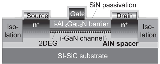
Figure 1: Schematic cross-sectional structure of AlGaN/AlN/GaN HEMT fabricated employing Si ion implantation doping.
The source–drain regions were formed using 50keV 28Si ion implantation with a dose concentration of 1x10¹⁵/cm2, followed by a rapid thermal anneal in nitrogen for 5 min at 1150°C. During these processes, the wafer was covered with silicon nitride (SiN), deposited using plasma-enhanced chemical vapor deposition (PECVD). The source–drain electrodes consisted of titanium-aluminum that was annealed for 2 minutes at 600°C.
Isolation regions were then formed using a multi-stage zinc ion implant, followed by application of the nickel-gold Schottky gate electrode. The final SiN passivation layer was applied using catalytic chemical vapor deposition.
Hall and transmission-line method (TLM) measurements were made to extract the characteristics of the 2DEG and ohmic contacts, respectively (Table 1).
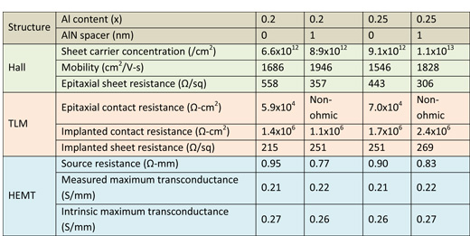
Table 1: Comparison of Hall characteristics, ohmic characteristics, and transconductance of four samples.
As expected, the insertion of the AlN spacer increases 2DEG carrier concentration and mobility with a 20% Al barrier. In fact, the carrier concentration is equivalent to that of a 25% Al barrier without spacer. In both cases, the increased amounts of carriers are attributed to polarization effects resulting from growing high-aluminum-content layers on the GaN buffer.
Increased Al-content of the barrier, however, reduces mobility due to alloy scattering and interface roughness effects. Insertion of the AlN spacer is effective at ameliorating alloy scattering effects in the 2DEG.
Without implanted source–drain regions, the AlN spacer makes for non-ohmic contacts due to the increased potential barrier from the very wide energy bandgap of the material (~6eV). Implantation of Si created comparable ohmic behavior for all epitaxial structures, and reduced contact resistance for material without AlN spacers.
Apart from silicon being a donor of electrons in nitride semiconductors, another effect of implantation – destruction of the layer structure with indistinct boundaries being produced – was seen under scanning electron microscopy (SEM). The structure alteration of mixing the AlN with the surrounding GaN and AlGaN layers is thought to reduce the potential barrier.
The researchers comment: “Because this mixed layer structure might almost be the same as the no-spacer structure with Si ion implantation doping, similar excellent ohmic characteristics, as mentioned before, could be obtained in spite of the AlN spacer layer insertion.”
In terms of the Schottky gate, it is found that, while the reversed-bias performances were similar across the devices, the AlN spacer reduced forward currents substantially. The reduced forward current was attributed to an increased band discontinuity at the heterointerface due to polarization effects. The gate leakage in the devices without AlN spacer increased significantly above gate voltages of +3V.
The HEMTs that were tested had gate length and width of 1μm and 50μm, respectively. The gate–source and gate–drain distances were 1μm and 2μm.
 The devices with AlN spacer and high-Al-content barriers had lower threshold voltages (i.e. more negative). The measured and intrinsic (i.e. minus contact resistance effects) transconductances were similar (Table 1). This is taken as an indication by the researchers that the saturation velocity of the 2DEG is not improved by the AlN spacer.
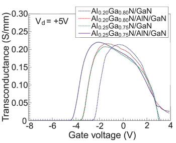
Figure 2: Gate voltage dependences of transconductance at drain voltage of +5V for the four HEMTs fabricated with Si ion implantation doping.
However, the transconductance is high over a wider region with an AlN spacer, and there is a tail into the region with gate voltages above +3V (Figure 2). Also, the maximum drain current at a gate voltage of +4V was 25–30% greater than without an AlN spacer. The researchers comment: “The obtained maximum drain current density was 1.3A/mm, which is sufficiently competitive with other reported values for AlGaN/AlN/GaN HEMTs. It should be noted that we could not have obtained these favorable results had the Si ion implantation doping not been employed in the fabrication of the HEMTs.”
Breakdown performance was not affected by the AlN spacer – all devices tested at a gate voltage of –5V had increasing drain current (more than the gate current) beyond 50V drain bias, and breakdown occurred at about 150V. “We consider that these breakdowns occurred as a result of the relatively large amount of residual impurities in the deep-channel-layer region or buffer layer in all of present four epitaxial wafers, which are not associated with the AlN spacer layer and Si ion implanted region.” All the devices also demonstrated similar current collapse effects in both DC and pulsed operation.
Nitride HEMTs grown on CMOS-compatible silicon
HEMT GaN AlGaN AlN spacer SiC substrates MOCVD PECVD
The author Mike Cooke is a freelance technology journalist who has worked in the semiconductor and advanced technology sectors since 1997.