- News
20 January 2011
Nitride solar cell achieves peak EQE of 72%
University of California Santa Barbara (UCSB) researchers have produced nitride semiconductor photovoltaic devices with external quantum efficiencies (EQE) of up to 72% [Elison Matioli et al, Appl. Phys. Lett., vol98, p021102, 2011]. One of the researchers, Claude Weisbuch, is also associated with Ecole Polytechnique in France.
Much of the nitride semiconductor work at UCSB concerns light-emitting devices. However, some of the researchers have previously (in 2008) reported photovoltaic (PV) devices that achieved an EQE of up to 63%.
Although these EQEs are impressive, one has to bear in mind that these devices cover only a small spectral range. In theory, nitride semiconductors could cover the wavelength range 200–2000nm, but this is limited at present by the ability to produce high-crystal-quality indium gallium nitride (InGaN) with high In content. Presently this becomes difficult with more than 20% In.
In both the latest work and the 2008 work, UCSB used InGaN with 12% In content. This restricts the effective performance of the devices to the wavelength range 370–410nm, which is a tiny sliver of the standard 1x sun (~1kW/m2) 1.5 air-mass (AM1.5G) illumination that is used as being representative of the spectrum at the Earth’s surface (Figure 1).
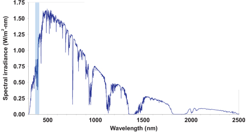
Figure 1: ASTM G173-03 AM1.5G reference spectrum. Shading represents effective response of UCSB device (370–410nm).
The active region of the devices (Figure 2) consisted of undoped indium gallium nitride (InGaN) with 12% In content. The active layer was 60nm thick and was grown at 880°C. All the nitride semiconductor layers were grown using metal-organic chemical vapor deposition (MOCVD).
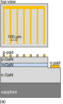 Figure 2: Schematic of UCSB InGaN/GaN solar cell structure.
The n- and p-type layers were achieved using silicon and magnesium doping, respectively. High levels of doping ([Si] ~ 6x10¹⁸/cm3, [Mg] ~ 8x10¹⁹/cm3) were used to counteract the effects of the polarization fields that normally degrade photovoltaic performance in nitride semiconductors. These fields act in an opposite sense to that of the diode depletion field and are in the same sense as is given by forward bias. The high doping helps to screen the polarization fields.
Surface roughening was used to increase the coupling of light into the device. This was achieved through the growth temperature. Two devices with different levels of surface roughness were produced. Growing the p-GaN layer at 880°C resulted in a root-mean-square (RMS) surface roughness of 7nm. Increasing the process temperature to 955°C gave a rougher surface of 41nm RMS. The metal contact grid consisted of palladium-gold, with 100μm spacing between lines.
The internal quantum efficiency (IQE) was derived from measurements of external quantum efficiency and light absorption. The EQE was that for 1x sun AM1.5G. The measurement was carried out in an Oriel solar simulator with xenon lamp illumination, and a monochromator was used to determine the spectral dependence. The absorption was determined using a Shimadzu ultraviolet–visible–near infrared (UV–VIS–NIR) system by combining reflected and transmitted light from unprocessed wafers in an integrating sphere.
The absorption measurement was carried out over 1cm2 of the sample, and devices were produced from this same area to ensure that the IQE determination (Figure 2) was ‘fair’. A total of 12 square devices were produced with various dimensions: 0.5x0.5mm, 1x1mm and 2x2mm.
In the GaN absorbing region with wavelengths shorter than 365nm (near UV), the external quantum efficiency is effectively zero because the photons are almost all absorbed in the p-GaN contact. The InGaN absorbing region covers wavelengths up to 410nm (violet).
The EQE follows the absorption curve closely in shape and magnitude in the InGaN absorption region (370–410nm). “This means that nearly all absorbed photons in this layer were converted into electrons and holes, and these charges were efficiently separated and transported out of the device,” the researchers comment.
The IQEs for both types of device were greater than 90%, with peak values of 97% (smoother surface) and 93% (rough surface). The researchers admit that they do not understand why the smooth device had a higher IQE, but suggest that it is due to run-to-run variations in the MOCVD growth process.
However, the rough device had a higher EQE of 72%, compared with 56% for the smoother device, due to the higher absorption of light. For example, the light absorption at 380nm was ~60% for the smooth device and ~80% for the rough device. A high EQE is required for practical devices.
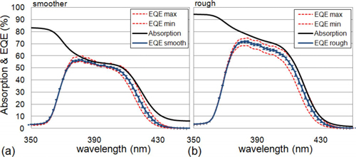
Figure 3: Measured absorption (solid), average (solid with error bars), maximum and minimum (dashed curves) EQE curves for (a) smoother and (b) rough samples. Average EQE and its standard deviation (error bars) were determined from measurements of 12 devices in the same area of the sample where the absorption was measured.
Further performance measurements were carried out to determine the standard performance metrics (Table 1) of open-circuit voltage (V{oc}), short-circuit current density (Jsc), maximum power (Pmax) fill-factor (FF = Pmax/V{oc}xJsc), and peak EQE and IQE.
Device |
Voc |
Jsc |
FF |
Pmax |
EQEpeak |
IQEpeak |
V |
mA/cm2 |
% |
mW/cm2 |
% |
% |
|
Smooth |
1.83 |
0.83 |
76.6 |
1.16 |
56 |
97 |
Rough |
1.89 |
1.06 |
78.6 |
1.57 |
72 |
93 |
Table 1: Solar cell performance metrics.
UCSB is not satisfied with the rough device absorption figure and suggests enhanced light coupling through “improved surface texture, by anti-reflecting and high-reflecting coatings in the top and bottom surfaces, respectively, or by coupling the incoming light to guided light using photonic crystals, which then can be fully absorbed by the active region”.
Free-standing GaN substrate improves nitride solar cell performance
Texas Tech ‘significantly’ improves InGaN solar cell performance
Nitride solar cell InGaN PV
The author Mike Cooke is a freelance technology journalist who has worked in the semiconductor and advanced technology sectors since 1997.