- News
7 February 2011
UCSB demonstrates record-frequency normally-off nitride transistor
University of California Santa Barbara (UCSB) has reported the first demonstration of high-frequency operation of N-polar enhancement-mode (normally-off) gallium nitride (GaN) transistors [Uttam Singisetti et al, Appl. Phys. Express, vol4, p024103, 2011].
The short-circuit current-gain cutoff (ft) for the UCSB device was 120GHz. Higher values of ft have been achieved for Ga-polar depletion-mode (normally-on) devices. For example, groups from HRL Laboratories/NASA’s Jet Propulsion Laboratory and MIT reported GaN high-electron-mobility transistors (HEMTs) with ft values beyond 200GHz at December IEEE International Electron Devices Meeting (IEDM 2010).
However, enhancement-mode devices are more attractive in terms of power efficiency, and a number of approaches are being developed to shift GaN transistor threshold voltages into enhancement. Using N-polar nitride semiconductors, rather than the more usual Ga-polar material, is one such approach and could lead to better carrier confinement in the channel.
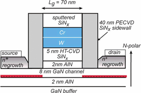 Although the 120GHz ft is promising, there are a number of less attractive features of the present device (Figure 1). First, the power-gain cut-off (fmax) for the same conditions was only 11GHz. The researchers attribute this to the high resistance of a thin tungsten (W) gate layer, commenting: “Incorporation of the top T-gate process would reduce the gate resistance, resulting in high ft and fmax simultaneously.”
Figure 1: Device cross-section schematic.
Further bad performance characteristics came in the form of poor saturation and high output conductance. These features need to be improved for use in analog circuits. The output conductance problem could be due to positively charged traps at the bottom aluminum nitride/gallium nitride (AlN/GaN) interface beneath the channel. Short-channel effects due to the low ratio (4.6) of gate length to gate-to-2DEG (two-dimensional electron gas) distance are also likely to be involved in the high output conductance. The self-aligned drain formation also leads to a higher drain voltage at the edge of the transistor’s active region. The researchers are presently working on these issues.
The on-resistance (2.6mΩ-mm) is also higher than previous N-polar devices developed at UCSB. This is ascribed to un-optimized re-growth conditions and sidewall access. The researchers believe that reduced silicon nitride (SiN) surface scattering and thinner sidewalls could help to improve the on-resistance by reducing sidewall contribution to the source access resistance.
The researchers conclude: “The future devices have to be optimized for low output conductance by further vertical scaling of the channel and the gate dielectric, and also by the optimization of the back barrier design. The growth and structures will also have to be optimized to reduce surface scattering in order to maintain high mobility in the sidewall access regions.”
The devices (Figure 1) were grown using plasma-assisted molecular beam epitaxy (PA-MBE) on a carbon-face silicon carbide (SiC) substrate. The device has an AlN back-barrier. The enhancement-mode behavior is created through an electric field in the channel induced by the polarization of the AlN capping layer.
The source/drain access to the channel was created by etching through the AlN cap. A chromium-tungsten-silicon nitride metal-insulator gate stack was then deposited and patterned using electron-beam lithographic techniques. The gate length was 70nm. The SiN was deposited using high-temperature chemical vapor deposition (HT-CVD). SiN gate sidewalls were formed using plasma-enhanced CVD (PECVD).
The source–drain contact regions consisted of 40nm indium gallium nitride (InGaN) graded to 10nm indium nitride (InN). These regions were highly doped for n-type conduction.
The threshold voltage of the device decreases with increasing drain current due to drain-induced barrier lowering (DIBL). At a drain bias of 3V, the peak drain current is 0.74A/mm and the peak transconductance is 260mS/mm, respectively. With zero gate voltage, the three-terminal breakdown voltage is 12V.
Small-signal frequency characterization (Figure 2) resulted in the extrapolated current-gain cut-off (ft) of 120GHz (pad de-embedded value) at a gate voltage of 2.5V and a drain bias of 3.0V. The researchers comment: “To the best of our knowledge this is the highest reported ft for E-mode GaN devices.”
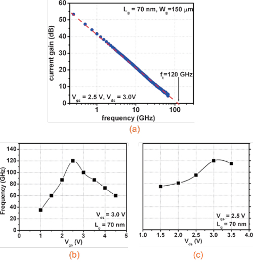
Figure 2: (a) Measured short-circuit current-gain (h21) versus frequency of device. A current-gain cut off frequency (ft) of 120GHz is extrapolated. (b) ft versus gate voltage for drain bias 3.0V, and (c) ft versu. drain bias for gate voltage 2.5V.
The work had financial support from the US Defense Advanced Research Projects Agency—Nitride Electronic Next Generation Technology (DARPA-NEXT) and Office of Naval Research—Millimeter-wave Initiative in Nitride Electronics multi-university research initiative (ONR-MINE-MURI) programs.
Normally-off nitride semiconductor tunnel junction FET with high drive
Normally-off GaN transistors PA-MBE SiC substrates AlN
The author Mike Cooke is a freelance technology journalist who has worked in the semiconductor and advanced technology sectors since 1997.
Join Semiconductor Today's group on LinkedIn