- News
28 February 2011
Monolithic InGaAs nanolaser on silicon
University of California at Berkeley (UCB) has produced III-V indium gallium arsenide (InGaAs) nanolasers monolithically integrated with silicon [Roger Chen et al, Nature Photonics, published online 6 February 2011]. Along with many other research groups, the UCB team is seeking to marry light emission and detection technology with mainstream silicon-chip-based electronics.
“Ultimately, this technique may provide a powerful and new avenue for engineering on-chip nanophotonic devices such as lasers, photodetectors, modulators and solar cells,” says the study’s lead author Roger Chen, a UC Berkeley graduate student in electrical engineering and computer sciences.
“Today’s massive silicon electronics infrastructure is extremely difficult to change for both economic and technological reasons, so compatibility with silicon fabrication is critical,” adds principal investigator Connie Chang-Hasnain, UC Berkeley professor of electrical engineering and computer sciences.
At the present stage, the UCB nanolasers are optically pumped using an external titanium-doped sapphire (Ti:sapphire) laser. However, electrically pumped lasers would be needed for the target of combining electronics with light-handling systems such as optical data links. Such links are being sought to overcome the limitations of chip-scale data transport around superfast microprocessors, along with longer distances (board-board, rack-rack, etc).
“In the future, we expect to improve the characteristics of these lasers and ultimately control them electronically for a powerful marriage between photonic and electronic devices,” says Chang-Hasnain.
The researchers believe that their core–shell nanopillar structure could be extended to give layers of n-, intrinsic (i-), and p-type material. Also, quantum wells could be arranged with layers of different alloy compositions.
Until now, III-V integration with silicon electronics has tended to be in the form of wafer bonding processes that generally have low yield of working devices. The alternative of making silicon light up is hindered by the indirect bandgap of silicon, which means that the material is a very inefficient emitter.
Problems in integrating III-Vs with silicon include lattice mismatching and high growth temperature. The lattice mismatch means that it is difficult to grow high-quality crystalline material. The high growth temperature creates problems for integration with silicon electronic devices, which suffer from degradation at elevated temperatures.
“Working at nanoscale levels has enabled us to grow high-quality III-V materials at low temperatures, such that silicon electronics can retain their functionality,” says Chen.
The UCB approach is to grow small III-V nanopillar structures ‘bottom up’, meaning that no special catalysts or ‘top-down’ structuring (e.g. lithography/etching) are used. Catalyst materials tend to be ‘poisons’ to silicon circuitry. An additional advantage of bottom-up processes is smooth crystal surfaces, avoiding the etch damage of top-down approaches. Rough surfaces would result in scattering losses. The symmetrical hexagonal shape resulting from the basic wurzite crystal structure of the InGaN also allows true single-mode oscillation.
The nanopillars consisted of an indium gallium arsenide (InGaAs) core and a gallium arsenide (GaAs) shell (Figure 1). After surface preparation, the pillars were grown in an Emcore metal-organic chemical vapor deposition (MOCVD) reactor. Before the growth, in-situ annealing was carried out for three minutes at 600°C. The growth temperature was 400°C, about 200–300°C lower than those typical for III-V materials.
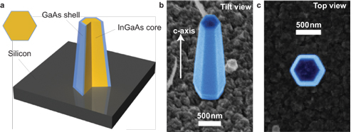
Figure 1: InGaAs/GaAs heterostructure nanopillar lasers monolithically grown on silicon: a, schematic of nanopillar laser monolithically integrated onto silicon (inset: top-view schematic); b, SEM showing well-faceted geometry of nanopillar optical cavity; c, top-view SEM.
The precursor gases were tertiarybutylarsine (TBA, also present during anneal), triethylgallium (TEGa) and trimethylindium (TMIn). The core growth lasted 60min. This was followed by the shell growth step.
Various indium compositions were used in the core: 12%, 15% and 20%. The shell thickness was also varied, with a 90nm shell used for room-temperature (293K) laser experiments and a thinner 30nm shell used at low temperature (4K). The thicker shell is needed for room-temperature operation to suppress surface recombination.
The nanopillars were vertical on the (111)-oriented silicon wafer substrates used. However, silicon electronics devices are usually grown on (100) silicon, where these nanopillars would grow on exposed (111) facets at an angle (54.7°) to the surface normal. Simulations suggest that such angled nanopillars could still support lasing at up to 70° tilt.
The grown nanopillars cover an area of about 0.34μm2 and are tapered with a 5° angle typical between opposite sidewall facets. The structures provide natural optical cavities, ‘supporting unique resonances that have not been observed before, to the best of our knowledge,’ the researchers report.
The excitation with a mode-locked Ti:sapphire laser exhibits ‘clear threshold behavior’ at room temperature with a ~950nm (near-infrared) laser oscillation from the 20%-In nanopillars. Shorter wavelengths (~50nm) are achieved with lower-In-content InGaAs pillars. The researchers say that they expect to be able to push the wavelengths of their devices into the silicon transparency region (> 1100nm), allowing transmission along silicon waveguides. Another possibility would be to use silica waveguides that are transparent at the demonstrated wavelengths, allowing low-cost silicon photodetectors to be used.
Low-temperature studies of the structure gave a cavity quality factor of 206 and a spontaneous emission factor of 0.01. The spontaneous emission factor measures the amount of emission coupled into the cavity mode of interest for lasing. The value is considered to be ‘reasonable’, given the small volume of the nanopillar (6x10-13cm3).
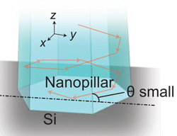 The researchers believe that the laser action is possible because the radiation is coupled into helically propagating cavity modes that reflect from surfaces at a shallow angle (Figure 2). The shallow angle means that the small index contrast between the InGaN nanopillar (3.7) and silicon substrate (3.6) is sufficient to provide the optical feedback that is needed (as indicated by the Q-value of 206). The grazing angle also overcomes absorption effects in silicon that are non-negligible at ~950nm.
Figure 2: Schematic depicting how a helical ray path enables reflection from a low-index-contrast interface due to glancing angle incidence.
The US Defense Advanced Research Projects Agency (DARPA) and a Department of Defense National Security Science and Engineering Faculty Fellowship helped to support the research.
The author Mike Cooke is a freelance technology journalist who has worked in the semiconductor and advanced technology sectors since 1997.
Join Semiconductor Today's LinkedIn networking and discussion group