- News
22 February 2011
Ge doping used for strain engineering control in GaN-on-Si
GaN-based epitaxy on silicon (Si) is very challenging because of the thermal mismatch between gallium nitride and silicon, which causes extreme tensile stress after cooling. However, professor Alois Krost and his team at the Otto-von-Guericke University in Magdeburg, Germany have applied an EpiCurveTT tool from LayTec of Berlin, Germany (which provides in-situ optical metrology systems for thin-film processes) to develop a new in-situ strain engineering method by using germanium (Ge) as the n-dopant instead of silicon (A. Dadgar et.al., ‘Crack-Free, Highly Conducting GaN Layers on Si Substrates by Ge Doping’, Applied Physics Express 4 (2011) 011001).
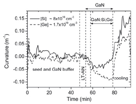 Figure 1: In-situ curvature measurements with EpiCurveTT of GaN/Si with Si doping (solid line) and Ge doping (dashed line).
Figure 1 shows curvature measurement on two differently doped GaN/Si samples. The downward slope after the low-temperature aluminum nitride (LT-AlN) interlayer growth indicates compressive stress. With the addition of Si as dopant, the slope inverts (solid line), the Si doping causes tensile stress and, during cooling, the sample cracks. In the case of Ge doping, however, the curvature slope remains unchanged (dashed line) and the sample remains crack-free.
Photoluminescence spectra of the Ge-doped GaN shows a doubled luminescence intensitiy compared with the Si doping. This proves good material quality of the approximately 1.6μm-thick GaN structure, says LayTec.
“The idea to dope GaN-on-silicon with an alternative dopant is quite old,” according to Armin Dadgar of Otto-von-Guericke University. “But now, with strain control and engineering with mixed dopants, EpiCurveTT gives a new impulse for GaN/Si device applications.”
* LayTec says that, at the end of 2010, more than 1200 of its metrology systems were in the field at customer sites. As one of Germany’s fastest-growing technology companies according to Deloitte’s ranking, last year the firm further increased its growth rate.
With the introduction of a new enterprise resource planning system (ERP), all key processes at LayTec have been streamlined, and quality management has been further improved to levels well above the established standards in semiconductor industry, the firm reckons. While production capacity was more than doubled in 2010, order lead-time were reduced by 30%, notes LayTec.
Ge doping alternative for GaN on Si
LayTec EpiCurveTT GaN-on-Si Ge doping
Join Semiconductor Today's LinkedIn networking and discussion group