- News
23 February 2011
Taking the a-plane to higher crystal quality
Taiwan’s Kun Shan University of Technology has developed a method to improve the crystal quality of a-plane gallium nitride (GaN) grown on r-plane sapphire [Hsiao-Chiu Hsu et al, Appl. Phys. Express, vol4, p035501, 2011]. The researchers used a modified one-sidewall-seeded epitaxial lateral overgrowth (OSELOG) method that reduces threading dislocation densities down to 106/cm2.
A further attraction is a coalescence thickness of less than 5μm, which is about half that of previous attempts using OSELOG. The researchers believe that the quicker coalescence offers opportunities for higher-throughput processes for crystal quality enhancement (i.e. higher productivity).
Normal c-plane nitride semiconductor LEDs suffer from polarization electrical fields in the active region generated from the ionic nature of the chemical bond between the group III metal (e.g. Ga) and nitrogen atoms. Although some of the polarization field is spontaneous, nitride semiconductors suffer particularly from strain-dependent piezoelectric effects. In light-emitting devices, these fields tend to hold the electrons and holes apart, disrupting their recombination as light. This effect is known as the quantum-confined Stark effect (QCSE).
In the past few years, a number of research groups have been investigating using nitride semiconductors that are oriented in non-polar or semi-polar crystal directions to reduce or eliminate QCSE. Such work has enabled laser diodes with longer-wavelength emission (green) and LEDs with a number of attractive features. Material oriented in these non-standard directions tends to have lower material quality than mature c-plane GaN.
The main non-polar direction material that has been researched in this way is labeled ‘m-plane’. However, there is another non-polar direction, ‘a-plane’. This material can be grown on r-plane sapphire substrates using metal-organic chemical vapor deposition (MOCVD). Unfortunately, the resulting crystal contains large numbers of threading dislocations (TDs ~1010/cm2) and basal-plane stacking faults (BSFs, ~105/cm).
Despite these problems, some groups have reported a-plane devices. In 2008, Rensselaer Polytechnic Institute and Kyma Technologies used a-plane material to create green LEDs with small blue-shift at high current density [Theeradetch Detchprohm et al, Appl. Phys. Lett., vol.92, p241109, 2008, http://link.aip.org]. In that case, the a-plane was cut from free-standing c-plane GaN that had been grown using hydride vapor phase epitaxy (HVPE; this method is also used to produce m-plane and semi-polar GaN pieces, for example, by University of California Santa Barbara and Mitsubishi Chemical).
Cutting non-polar or semi-polar material from free-standing c-plane GaN material restricts the size of substrates by the thickness of the HVPE growth process. Hence, growing a-plane GaN on r-plane sapphire is attractive if the quality can be increased in a relatively simple, time- and money-efficient manner.
More recently, researchers associated with a variety of Korean organizations (Kongju National University, THELEDS Co Ltd, Korea Electronics Technology Institute, Chungnam National University, Wavesquare Inc) have reported Raman and emission properties of a-plane LEDs grown on r-plane sapphire [Yanqun Dong et al, J. Appl. Phys., vol.109, p043103, 2011, http://link.aip.org]. Although the a-plane device had lower maximum external quantum efficiency (EQE) than a comparison c-plane LED, the a-plane device maintained its EQE to higher currents (reduced ‘droop’). Presumably, higher-quality a-plane GaN would exhibit higher EQEs.
The Kun Shan researchers began their a-plane OSELOG with r-plane sapphire prepared with GaN stripes to act as seeds for the a-plane material. The stripes are formed using a silicon dioxide (SiO2) mask formed lithographically on a layer of a-plane GaN material. The windows in the SiO2 layer are then etched down to the sapphire. The ‘wing’/seed under the SiO2 was 2μm wide and the windows were 1.6μm.
Since the seed is a-plane oriented, the c-planes are ‘vertical’ (rather than ‘horizontal’ as in c-plane material; the [0001] c-direction is ‘horizontal’ with a-plane, and ‘vertical’ with c-plane) and the sidewalls of the stripes can be arranged to be Ga- and N-face.
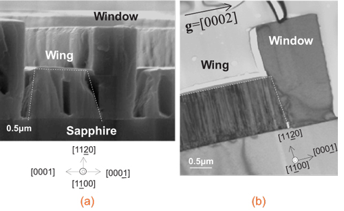
Figure 1: Cross-sectional SEM and TEM images of a-plane GaN after first step of GaN growth with V/III growth rate ratio of 1000. The SiO2 is removed for the SEM.
The re-gowth on the seed layer proceeds by supplying precursors (ammonia, trimethyl-Ga) with a high V/III (N/Ga) ratio of 1000 to encourage growth from the N-face (Figure 1). The V/III ratio is then reduced to 220, making the N-face and Ga-face sidewall growth rates nearly equal. This ratio was maintained until the GaN coalesced over the SiO2 mask (Figure 2).
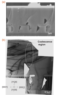 Figure 2: Cross-sectional SEM and TEM images of fully coalescence a-plane GaN after second step with V/III growth rate ratio of 220.
This process was carried out with various trimethyl-Ga (TMGa) flow rates (15, 30 and 45 standard cubic centimeters, ‘sccm’) in the second step with V/III ratio 220. An ‘as-grown’ (i.e. no overgrowth) a-plane GaN sample with a similar layer thickness was used as a reference in the crystal quality characterization.
Measurements on the OSELOG material suggest that the dislocation density over the window regions was 3–4 orders of magnitude (factors of 10) lower than over the SiO2 ‘wings’.
Air voids formed near the SiO2 mask due to the different shapes of the Ga- and N-face growth profiles — for example, the Ga-face growth tended to have an arrow-head shape with [11–2n] facets. However, the exact form depends on the exact growth conditions (temperature, V/III ratio, hydrogen carrier flow rate, etc.). The researchers believe these voids do not affect material quality and may even be beneficial in relaxing strain as the temperature is reduced to room temperature after growth.
The coalescence over the SiO2 mask occurred earlier (after 3.9μm) than with the previous report (10μm) of a-plane OSELOG material from Meijo University in Japan. Adding in the as-grown seed layer, the total thickness of the Kun Shan samples were 5.5μm. The quicker coalescence and hence reduced overall thickness is attributed to ‘optimum growth conditions and narrower stripes’.
The Kun Shan researchers comment: ‘The result indicated that the modified OSELOG approach is able to reduce the process time and improve the yield when compared with the conventional ELOG technology.’
Apart from electron microscopic inspection, the materials were also characterized using x-ray diffraction (XRD) and low-temperature (11K) cathodo-luminescence (CL; light excited by an electron beam). The XRD scans were carried out along the c-axis and m-axis (Table 1), and the results suggest improved crystal quality for the 30sccm TM-Ga flow.
TM-Ga flow (sccm) |
As-grown |
15 |
30 |
45 |
c-axis |
0.398 ° |
0.379 ° |
0.141 ° |
0.387 ° |
m-axis |
0.527 ° |
0.301 ° |
0.110 ° |
0.199 ° |
Table 1: Results for XRD ω-scans along c- and m-axes.
The CL spectral measurements over a 20μm x 20μm area were used to assess the various defects using emissions from donor-bound excitons (D0X, 3.472eV), BSFs (3.417eV) and donor–acceptor pair (DAP, 3.345–2.8eV) recombination.
The Kun Shan researchers interpret their CL results as showing that the TM-Ga flow rate controls the strain in the GaN epilayer. The strain condition affects the tendency to form defects. Low defect levels are needed to create efficient light-emitting devices.
Again, the lowest level of BSF emission, relative to the D0X signal, is seen in the middle-range TM-Ga flow of 30sccm (BSF/D0X ratio 1.74, compared with 2.15 for 15sccm and 3.54sccm for 45sccm). The DAP emissions provided information about silicon and oxygen donor effects due to decomposition of the SiO2 mask, along with defect distributions.
GaN a-plane GaN Sapphire substrates
The author Mike Cooke is a freelance technology journalist who has worked in the semiconductor and advanced technology sectors since 1997.
Join Semiconductor Today's LinkedIn networking and discussion group