- News
10 February 2011
Normally off nitride transistor with oxide insulated gate
Researchers in Japan have developed normally-off nitride semiconductor high-electron-mobility transistors using an electrochemical oxidation process [Naohisa Harada et al, Appl. Phys. Express, vol4, p021002, 2011]. The team consisted of scientists from the Graduate School of Information and Science Technology and Research Center for Integrated Quantum Electronics (RCIQE), Hokkaido University, and the Japan Science and Technology Agency Core Research of Evolutional Science & Technology (CREST) organization.
Nitride semiconductor HEMTs are being developed for high-power and high-frequency handling applications such as power amplification of radio transmission signals, power management and power switching.
Normally-off behavior is desired from the perspectives of low power consumption and for fail-safe reasons in power switching devices.
 Much work has recently been carried out using various techniques to achieve normally-off behavior in aluminum gallium nitride (AlGaN) HEMTs. As-grown nitride HEMTs tend to have normally-on behavior, where a gate potential is needed to turn off current flow through the channel.
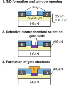
The researchers grew AlGaN/GaN heterostructures on sapphire (Figure 1), using metal-organic chemical vapour deposition (MOCVD). The source and drain contacts consisted of metal multi-layers (titanium-aluminum-titanium-gold), annealed for 1 minute at 800°C in nitrogen.
Figure 1: Fabrication process of recessed-oxide-gate AlGaN/GaN HEMT by selective electrochemical oxidation.
The selective oxidation was carried out using a 100nm silicon dioxide mask. The oxidation window was patterned lithographically and wet etched in a buffered hydrogen fluoride solution. The electrochemical oxidation used an electrolyte consisting of propylene glycol and tartaric acid (3% by weight). A neutral pH of 7.0 was achieved by adding ammonium hydroxide (NH4OH).
Platinum was used as cathode, and the drain as common electrode. A silver–silver chloride reference electrode was used to control the potential at the AlGaN surface. The oxidation reaction desired was:
2GaN (2AlN) + 6h+ (holes) + 6OH- → Ga2O3 (Al2O3) + 3H2O + N2↑
The holes were supplied to the reaction through ultraviolet (UV) illumination (25mW/cm2, 300–400nm wavelength) of the oxide/AlGaN interface. Initially the oxidation reaction is rather slow because the generated holes are swallowed up by the two-dimensional electron gas (2DEG) at the AlGaN/GaN interface. However, after a few minutes the rate increases due to depletion of the 2DEG, which allows more of the holes generated by the UV illumination to participate in the oxidation.
The resulting oxide layer is amorphous. A 260 second oxidation resulted in a 7nm oxide layer. The researchers describe the AlGaN/oxide interface as being ‘relatively flat’, adding: “The flatness and uniformity of the electrochemical oxide layer is much better than those by dry oxidation at high temperatures”. Atomic force microscopy (AFM) measurements gave a root-mean-square roughness for the oxide surface of 1.3nm.
X-ray photoelectron spectra (XPS) studies revealed that the Ga and Al energy levels were close to those seen in Ga2O3 and Al2O3. The composition ratio of the two components followed that of the original AlGaN alloy layer.
The final gate electrode consisted of nickel-gold, deposited after the oxidation process.
The researchers produced recessed oxide-gate and normal Schottky gate HEMTs with a gate length of 12μm and a source–drain spacing of 30μm. The oxide thickness was 20nm, measured using transmission electron microscopy (TEM). The gate control of both devices was similar. However, the oxide-gate device had a normally-off behavior.
The oxide-gate device had a relatively high contact resistance for the source–drain electrodes, degrading linearity at low drain bias. The researchers think that the contact resistance problem is probably due to ‘a fluctuation of process condition’.
On the plus side, the gate leakage (Figure 2a) is much reduced by the presence of the oxide layer. At a gate potential of 2V, the leakage is nine orders of magnitude less than for the reference device with Schottky gate. The increase in leakage above this potential for the oxide HEMT is blamed on Fowler–Nordheim tunneling through the oxide.
HEMT devices with 10nm oxide were also produced. This device had a similar transfer curve shape to the Schottky device (Figure 2b). The researchers believe that more ohmic source–drain electrodes for the 20nm oxide HEMT would result in a curve with a similar steepness to the 10nm oxide and Schottky HEMTs. The threshold voltage for the 20nm device was +1.2V.

Figure 2: (a) Gate leakage and (b) transfer characteristics of reference Schottky-gate and recessed-oxide-gate HEMTs.
The researchers suggest that in-situ monitoring of the conductance between the source–drain electrodes during oxidation could lead to more precise control of the HEMT threshold. Further work is needed to characterize the stability and reliability of these devices.
UCSB demonstrates record-frequency normally-off nitride transistor
Normally-off nitride semiconductor tunnel junction FET with high drive
Normally-off HEMT AlGaN/GaN MOCVD
http://apex.jsap.jp/link?APEX/4/021002
The author Mike Cooke is a freelance technology journalist who has worked in the semiconductor and advanced technology sectors since 1997.
Join Semiconductor Today's group on LinkedIn