- News
14 December 2011
Quantum well steps to efficient multi-junction solar cells
University of Tokyo researchers have been investigating the application of quantum well technology to solar cells based on indium gallium arsenide phosphide (InGaAsP) semiconductors [Yu Wen et al, Appl. Phys. Express, vol4, p122301, 2011]. In particular, they found that inserting GaAs step layers between the quantum wells and barriers improved the short-circuit current of the devices.
Indeed, a device with 20 quantum wells (QWs) had a current density of 20.25A/cm2 under 1 sun air-mass 1.5G (AM1.5G) illumination. For 10 QWs, the current density was 19.29A/cm2. A comparison device with no quantum wells had 18.80A/cm2 short-circuit current density under the same conditions. Thus the 10-well device, which was of a similar thickness to the comparison device, had 14% more current. The improvement in short-circuit current only degraded the open-circuit voltage significantly in comparison QW devices without the GaAs step structure (Table 1).
Sample |
QW stacks |
GaAs step |
Jsc (mA/cm2) |
Voc (V) |
FF (%) |
Efficiency (%) |
A |
20 |
Yes |
20.25 |
0.88 |
80 |
14.2 |
B |
10 |
Yes |
19.29 |
0.88 |
79 |
13.4 |
C |
10 |
No |
16.85 |
0.89 |
71 |
10.7 |
D |
N/A |
N/A |
18.80 |
0.97 |
82 |
14.9 |
Table 1: Characteristic structure and performances of QW cells.
The researchers see MQW devices as having application in tandem solar cells that use multiple junctions to extract energy from different energy bands of light. One problem with such devices is that the current running through all the junctions has to be matched for high conversion efficiency.
This is a particular problem for InGaP/GaAs/germanium designs. It is hoped that, by using semiconductor nanostructures such as quantum wells, the currents can be tuned to match with other junctions in the structure. One disadvantage of quantum wells is that they can trap carriers, thereby allowing them to recombine either by re-emitting light or through other non-radiative mechanisms.
 These trapping effects such as increased dark current and reduced open-circuit voltage can be minimized by strain-balancing. The Tokyo GaAs-step is designed to create an escape route for photo-generated carriers, reducing recombination in the wells. The step structure is also combined with strain compensation to allow a large number of wells to be created.
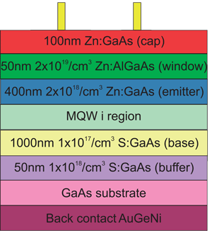
Figure 1: Schematic structure of QW solar cells.
The strain compensation is achieved through careful design of the composition and thickness of the InGaAs wells (16% In, 7.6nm), GaAs steps (2x8nm) and GaAsP barrier (21% P, 11.6nm). The step layers also improve the material quality of the structure, as confirmed in atomic force microscope (AFM) and x-ray studies.
Four structures were tested (Table 1): sample A with a 20-period multi-quantum well (MQW) including GaAs step; sample B with a 10-period MQW with GaAs step; sample C with 10-period MQW without GaAs step, but with an extra 160nm intrinsic GaAs layer; and, sample D, a reference cell with no QWs but 350nm intrinsic GaAs. The three last devices had roughly comparable active regions in terms of thickness (~350nm).
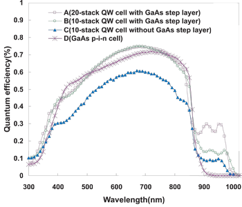 Figure 2: External quantum efficiencies.
The structures (Figure 1) were grown on GaAs substrates using metal-organic chemical vapor deposition (MOCVD). The epitaxial material was processed into small mesa-type devices with a 1mm-diameter circular active region. No anti-reflective coating was applied. The p-contacts were titanium/gold.
In terms of spectral response (Figure 2), all the devices responded to radiation with photon energies above the GaAs bandgap – i.e. wavelengths shorter than 870nm. However, the devices with QWs also responded to longer wavelengths up to 1000nm. Device C, without GaAs-step, had reduced response in both regions, compared with A and B. The responses for A and B were comparable to that of D above the GaAs bandgap.
Multi-junction solar cells GaAs solar cells Quantum wells InGaAsP GaAs substrates
The author Mike Cooke is a freelance technology journalist who has worked in the semiconductor and advanced technology sectors since 1997.