- News
31 December 2011
Developing monolayer graphene for transparent conduction in nitride semiconductor LEDs
Korean and US researchers have compared the performance of graphene as a transparent conducting electrode (TCE) on the p-contact of nitride semiconductor light-emitting diodes (LEDs) with indium tin oxide (ITO) [Tae Hoon Seo et al, Jpn. J. Appl. Phys., vol50, p125103, 2011]. The latter material is commonly used for this purpose in LEDs and solar cells.
One particular attraction for graphene is that it transmits light of shorter wavelengths beyond the 300–400nm ultraviolet range where ITO cuts off. Comparisons between the light transmittance of graphene and 250nm-thick ITO on aluminum oxide in the wavelength range 400–800nm gave values of more than 90% (up to nearly 97%) and ~80%, respectively. Below 400nm (the ultraviolet region), graphene continued to transmit ~90% light, while ITO became opaque around 300nm.
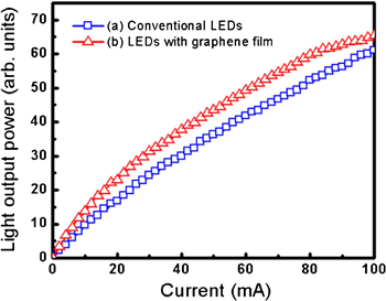 One drawback of graphene is that it is more resistive than ITO. This means that the forward voltage at 20mA of the graphene contact LED was 5.87V, compared with 3.4V for the ITO-based device. Despite this, the light output power was some 25% greater in the graphene LED at 20mA (Figure 1). The power loss of the graphene contact does begin to impact performance around 80mA, creating early saturation of the device performance.
Figure 1: Light output power of LEDs vs current.
The researchers expect further efficiency enhancements in GaN-based LEDs that use graphene due to the intensive research in graphene material. This research is expected to allow enhanced electrical properties such as control of the graphene work function and the reduction of sheet resistance.
The latest research (involving Chonbuk National University, University of Michigan, and Sungkyungkyun University) used monolayer graphene grown on copper foil. A couple of months ago a different team of researchers from Korea University, Korea Electronics Technology Institute and US Naval Research Laboratory reported the use of few-layer graphene as a TCE for UV applications (Graphene as transparent conductor for UV LED current spreading).
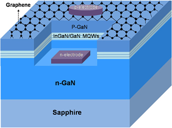
The new LED structures were grown on sapphire using metal-organic chemical vapor deposition (MOCVD). The active layer was a five-period InGaN/GaN quantum well/barrier structure. The p-GaN layer was 200nm thick. The n-GaN layer was 2μm thick, grown on a 2μm GaN buffer and 25nm GaN nucleation layers.
 The high-quality monolayer graphene was produced using chemical vapor deposition of 70μm copper foil. After a preparatory flow of hydrogen to reduce oxide on the copper (2.5 hours), the carbon source of methane was introduced (30mins). To transfer the graphene, a poly(methyl methacrylate) (PMMA) film was spin-coated on the graphene. The copper was then (wet) etched away. The graphene was then applied to the GaN surface and the PMMA removed by annealing at 500°C in a hydrogen/argon mix for 30mins.
Figure 2: Schematic diagram of GaN-based LEDs with graphene film.
The LEDs (Figure 2) were formed by creating a mesa, removing the graphene film in the n-electrode region using an asher, and then plasma etching the nitride semiconductor material down to the n-type layer. The electrodes for the n- and p-layers were chromium/gold. Devices with 250nm ITO transparent conduction layers were also produced for comparison.
Graphene as transparent conductor for UV LED current spreading
The author Mike Cooke is a freelance technology journalist who has worked in the semiconductor and advanced technology sectors since 1997.