- News
10 December 2011
Digital etching for damage-free gate recess in nitride transistors
RWTH Aachen University in Germany has produced aluminum gallium nitride (AlGaN) semiconductor heterostructure field-effect transistors (HFETs) on silicon with record performance [Herwig Hahn et al, Appl. Phys. Express, vol4, p114102, 2011]. In particular, the extrinsic transconductance was 420mS/mm and the maximum drain current was 500mA/mm. The threshold was +0.5V, allowing enhancement-mode/normally-off behavior that is desired for applications.
The results were achieved using a new etch technique that allows recessing of the gate into the barrier while not damaging the epitaxial material. The ‘digital etch’ technique can be seen as comparable to operating atomic layer deposition (ALD) in reverse. Like ALD, digital etch uses pulsed plasmas to increase control of the process.
The researchers processed standard commercial epitaxial wafers of AlGaN/GaN on (111) silicon substrates. The barrier layers consisted of 26%-Al AlGaN on an AlN mobility-enhancement layer, with 2nm GaN cap. The total barrier thickness was 17.4nm.
Processing began with a standard chlorine-based etch to create the isolation mesa. Ohmic contacts consisted of titanium-aluminum-titanium-gold alloyed at 825°C in nitrogen. A 120nm silicon nitride (SiN) passivation layer was added with plasma-enhanced chemical vapor deposition (PECVD). The SiN was also used to define the gate foot through lithography and fluorine-based plasma etch.
Using the SiN as etch mask, the digital etch was performed to create the recessing for the gate foot. The etch sequence consisted of alternating oxidation and boron-trichloride (BCl3) plasmas. The BCl3 etches oxide much faster than the underlying nitride semiconductor. The researchers describe the process as being ‘semi self-limiting’. “As a consequence, dead times at the beginning of an etch are eliminated and the etch rate control is improved,” they comment.
The digital etch was optimized to give minimal damage and an etch rate of 1nm/etch cycle. The root mean square (rms) roughness was 1.17nm before the etch and 1.20nm after. The gate was completed by depositing nickel-gold.
Three types of device were produced: without gate recessing (NR), or with shallow (6.3nm, SR) or deep (10.3nm, DR) recessing. These recessing types correspond to barrier thicknesses of 17.4nm, 11.1nm, and 7.1nm, respectively. The gate was 1μm long (Lg), with source–gate and gate–drain distances also each 1μm. The gate width was 2x50μm (i.e. the gate extended out 50μm on each side of a central feed line).
One effect of increasing the recess depth was to push the threshold voltage to positive values: without recessing the gate threshold at 3V drain bias was –1.0V; this increased to –0.1V for shallow recessing and reached +0.5V for deep recessing. The positive threshold gives the deep recessed transistor an enhancement-mode normally-off behavior.
Although the on-drain current was reduced for the deep recessed device to 500mA/mm from the 600mA/mm of the non-recessed and shallow-recessed devices, the researchers comment: “Nonetheless, this value is still the highest reported drain current for enhancement-mode AlGaN/GaN-on-Si HFETs”.
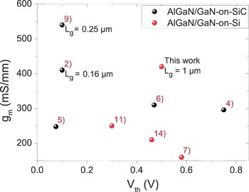
The maximum intrinsic transconductance for the non-, shallow- and deep-recessed HFETs were 265mS/mm, 363mS/mm, and 420mS/mm, respectively. The 420mS/mm value is described as “the highest value reported so far for enhancement-mode AlGaN/GaN-on-Si HFETs” and “very much comparable to the values from enhancement-mode HFETs on SiC with even lower Lg”. On the basis of these results, the researchers draw the conclusion that their process is nearly damage-free.
The off-state current is limited by gate leakage, with all devices showing similar behavior below a gate potential of –2V. “The extrapolated on/off ratios exceed four orders of magnitude, which is an excellent value for HFETs with a Schottky gate and without a backbarrier,” the researchers comment. A backbarrier would improve electron confinement in the channel, and hence would give a harder pinch-off. The researchers also observe no increase in off-current resulting from barrier thinning.
However, the turn-on voltage of the gate-diode is reduced by recessing, reducing in turn the maximum forward gate bias and maximum drain current (Id) of the deeply recessed device. The researchers comment: “The reduction in Schottky barrier height prevents a further increase in Id and, therefore, the addition of an insulating layer, forming a MIS-HFET device, is desirable.”
 Pulsed measurements were also carried out to assess current collapse: temporary drain current reductions due to surface and bulk carrier trapping. The results suggest improvements of more than 40% in current recovery after the pulse for both shallow- and deep-recessed devices, compared with no recessing.
Figure 1: Comparison of extrinsic transconductance versus threshold voltage for HFETs based on AlGaN/GaN-on-SiC (black squares) and AlGaN/GaN-on-Si (red triangles). The reference numbers refer to the original paper.
Comparing their results with other groups using silicon and silicon carbide substrates (see Figure), the researchers declare: “Our work represents a new milestone for Si-based AlGaN/GaN HFETs”. In view of the difference in gate length with the SiC devices shown, they add: “the devices demonstrated here are highly comparable to published results on SiC”.
The author Mike Cooke is a freelance technology journalist who has worked in the semiconductor and advanced technology sectors since 1997.