- News
29 December 2011
Back-barrier enhancements to AlN/GaN HEMTs
France’s Institute of Electronic, Microelectronic and Nanotechnology (IEMN) has added a back-barrier to its aluminum nitride-on-gallium nitride (AlN/GaN) high electron mobility transistors (HEMTs) to increase electron confinement and hence low subthreshold drain leakage beyond 50V [Farid Medjdoub et al, Appl. Phys. Express, vol4, p124101, 2011]. Further improvements include enhanced RF performance figures.
The researchers believe their technology could lead to cost-effective millimeter-wave high-power/high-linearity device applications.
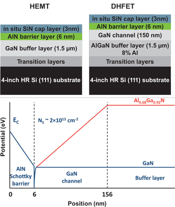 The heterostructures (Figure 1) were grown by the company EpiGaN on highly resistive 4-inch (111) silicon using metal-organic chemical vapor deposition. Two device types were compared: an ordinary HEMT and a new double heterostructure field effect transistor (DHFET). In-situ MOCVD silicon nitride was used as early passivation and to prevent strain relaxation.
Figure 1: Cross section of the fabricated AlN/GaN-on-Si HEMTs (top left) and DHFETs (top right) and schematic of the conduction-band diagram of the HEMT and the DHFET.
The GaN channel layer in the DHFET was grown thick enough to minimize the effect of the GaN/AlGaN back-barrier interface on the two-dimensional electron gas (2DEG) channel layer near the AlN/GaN interface. The Hall charge carrier concentration was 2.2x10¹³/cm2 for the HEMT structure and only slightly less at 2x10¹³/cm2 for the DHFET. The respective mobilities were 1200cm2/V-s and 1400cm2/V-s. These values resulted in sheet resistances of 235Ω/sq. and 240Ω/sq. for the HEMT and DHFET materials, respectively.
The ohmic source-drain contacts were titanium/aluminum/nickel/gold and the Schottky gate nickel/gold. The gate length was 0.2μm; the source- and drain-gate distances were 0.3μm and 1μm, respectively. The device width was 50μm. Nitrogen implantation was used to isolate devices. Further layers of plasma-enhanced chemical vapor deposited SiN were applied for more passivation.
The maximum output direct current density at gate potential 2V was 1.8A/mm for both the HEMT and DHFET. The researchers attribute the high current to the high sheet carrier density enabled by
using AlN instead of AlGaN for the top barrier. AlN has the highest spontaneous polarization of all the III-nitride semiconductor materials.
Total pinch-off occurs at gate potential of -4V. The DHFET has a slight shift in threshold voltage and a more pronounced thermal effect due to the lower thermal conductivity of the AlGaN back-barrier compared with the GaN buffer of the HEMT device. The transconductance of the two devices is almost identical at 470mS/mm under optimum bias conditions.
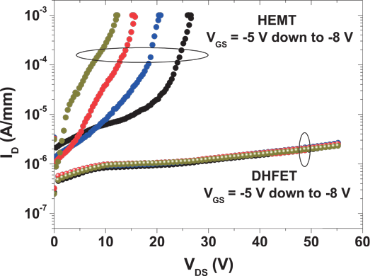
Figure 2: DC output for drain current vs. drain bias (ID–VDS) characteristics of 2x25μm AlN/GaN-on-Si HEMT and DHFET in subthreshold region. Gate potential (VGS) swept from -5 to -8V in 1V steps.
However, at high drain bias the single heterostructure AlN/GaN HEMT breaks down above 10V in terms of pinch-off of current (Figure 2). The AlN/GaN/AlGaN DHFET allows operation above drain bias of 50V, while still maintaining a subthreshold leakage of a few μA/mm.
The gate leakage for reverse bias is less than 10μA/mm for both device types down to -60V gate potential. The breakdown in the HEMTs is thus attributable to electron injection into the buffer layer and excludes the possibility surface leakage problems (that would show up as gate leakage).
The researchers comment: “For the DHFET, the AlGaN back barrier prevents the electron flow into the buffer under high drain bias, reducing the subthreshold drain leakage current and postponing the punch-through of the buffer layer.”
The frequency performance of the devices were also determined giving cut-offs (fT) of 44GHz and 52GHz for the HEMT and DHFET, respectively. Maximum oscillation (fmax) occurred respectively and 68GHz and 91GHz. The researchers write: “The reduction of the short-channel effect results in a slightly better fT and a decrease of the output conductance that involves a significant improvement of fmax.”
The researchers believe that reducing the DHFET gate length below 100nm (0.1μm) should “pave the way for higher frequency operation of GaN-based devices grown on highly resistive Si substrate combined with high power (e.g., high current density and high voltage).”
First noise assessment of AlN/GaN HEMTs on silicon
Combining high current with high transconductance
Record transconductance for nitride HEMT on silicon
AlN barrier increases output current from GaN/Si HEMTs
The author Mike Cooke is a freelance technology journalist who has worked in the semiconductor and advanced technology sectors since 1997.