- News
21 December 2011
First yellow-green and amber micro-LED arrays
University of Strathclyde, Peking University, and Epilight Technology Co., Ltd have made what they believe to be the first demonstration of yellow–green and amber III-nitride micro-LED arrays, based on new epitaxial structures [Z Gong et al, Semicond. Sci. Technol., vol27, p015003, 2012].
The researchers see applications for micro-LED arrays coming from scientific instrumentation, optical communications and micro-displays. The LED emissions can be tuned to the absorption lines of biological active molecules, allowing optogenetic experiments to be controlled in both time and space, for example. Optoelectronic tweezer (OET) control is another possibility.
Rather than using expensive non- or semi-polar nitride substrates, the epitaxial material was grown on standard (0001) sapphire using metal-organic chemical vapor deposition. Freestanding nitride substrates are particularly used for producing devices with longer wavelengths (green, yellow, amber, etc.), where reducing defects and polarization field effects are critical to performance.
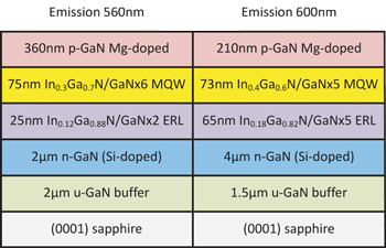 Different buffer and active layers of InGaN/GaN wells and barriers (Figure 1) were used in two device types emitting light of wavelengths 560nm (yellow-green) and 600nm (amber). The researchers used a low-indium-content InGaN/GaN electron reservoir layer (ERL) that is believed increase carrier capture in the QWs above, improving radiative efficiency.
Figure 1: Schematic epitaxial structures for yellow-green (560nm) and amber (600nm) micro-LED arrays.
It is also believed that use of an ERL makes the usual electron blocking layer (EBL) above the active layers unnecessary. EBLs are used to stop electrons overshooting the wells and from entering the p-type hole injection layers, reducing radiative efficiency.
To produce devices the epitaxial material was flipped so that light emission was through the polished sapphire substrate. The micro-LEDs consisted of 10x10 circular device arrays of 40μm diameter and 100μm pitch.
The mesas for the LEDs were created using inductive coupled plasma to etch down to the n-type layer. The current spreading p-contacts consisted of nickel/gold.
The n-contact of titanium/gold was formed in the space between the devices. Four n-contact electrode pads were created at the middle of each side of the square array for more uniform current spreading on the n-side of the device.
Silicon dioxide was used as electrical isolation, allowing titanium/gold p-metal buses to be deposited for electrical access to the p-contacts of individual pixels. The arrays were then bonded to printed circuit boards.
There is a large spectral blueshift to short wavelengths in main device peaks as the current injection increases in the devices. For the yellow-green LED the shift is around 45nm in moving up to 5.57kA/cm2 current density. There is also movement in light from the ERL (~450nm, blue), with the peaks initially blue-shifting to about 12nm at 0.6kA/cm2 and then red-shifting. The ERL peak is very small in the green-yellow device, but quite large at low current for the amber LED.
The researchers used simulations to explore the spectral shifting effects of screening by current injection of the quantum confined Stark effect from variation of the spontaneous and piezoelectric polarization fields (blue-shift), band-filling (blue-) and Joule heating (red-). They believe the screen effect dominates below 3.5kA/cm2, whereas band-filling accounts for further blue-shifts above that value.
 The researchers comment: “Further optimization of the epitaxial structures is feasible to suppress these spectral shifts, and the insights obtained from the simulations should help guide the design of more advanced epitaxial structures.”
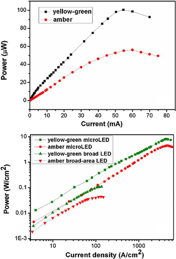
Figure 2: (a) Power outputs of yellow–green micro-LEDs and amber micro-LEDs as function of injection current; (b) power density vs. current density of yellow–green micro-LEDs and amber micro-LEDs. For comparison, power densities of conventional broad-area LEDs made from same wafer are also plotted.
The power output (Figure 2) of one pixel was measured by placing a silicon photodetector close to the sapphire surface, collecting the usable light in the upward direction. The calibration for the power measurement was over the 500-600nm range to allow for the spectral shift of the device. The peak power (thermal roll-over) was attained at 0.1mW and 55mA (4.4kA/cm2) for the yellow-green pixels and at 0.055mW and 60mA (4.8kA/cm2) for the amber pixels. These correspond to power densities of 8W/cm2 and 4.4W/cm2, respectively. Further characteristics can be found in Table 1.
Type of device |
V{on} |
Rs |
Maximum power per pixel |
Maximum power density |
Yellow–green |
3.2V |
360Ω |
100μW |
8.0W/cm2 |
Amber |
3.8V |
730Ω |
55μW |
4.4W/cm2 |
Table 1: Typical electrical and optical characteristics per pixel for yellow-green and amber LED arrays.
The researchers comment: “These power densities exceed by more than an order of magnitude the requirements typical for applications.”
The devices perform better than broad area devices. The researchers comment: “This is consistent with the numerical results of size-dependent self-heating that we have presented previously for LEDs emitting at 400nm where we showed the junction temperature in a smaller pixel to be much lower than that in a larger one under the same current density.”
The author Mike Cooke is a freelance technology journalist who has worked in the semiconductor and advanced technology sectors since 1997.