- News
30 August 2011
More positive threshold with Al2O3 and m-plane nitride semis
The USA’s University of California Santa Barbara (UCSB) and Japan’s Rohm Co Ltd have produced enhancement-mode (E-mode) nitride semiconductor heterojunction field-effect transistors (HFETs) with a threshold voltage of +3V and on/off current ration of 4x10⁶ [Tetsuya Fujiwara et al, Appl. Phys. Express, vol4, p096501, 2011]. Enhancement-mode, or ‘normally-off’, operation is seen as being particularly important for power switching devices because one wants such devices to switch off if they fail.
Nitride semiconductor HFETs (also known as high-electron-mobility transistors, HEMTs) usually operate in depletion-mode (‘normally-on’ at zero gate potential). A number of techniques have been used to shift the threshold in a positive direction, but the threshold voltage has fallen short of the +3V or more needed to choke off leakage currents at zero gate potential.
Most previous devices have used c-plane oriented crystal nitride semiconductor material where the difference in the c-direction polarization field between the gallium nitride (GaN) buffer and aluminum gallium nitride (AlGaN) barrier layers creates a two-dimensional electron gas (2DEG) at the AlGaN/GaN interface that carries current at zero gate potential.
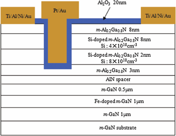 In 2009, UCSB researchers created an HFET with +2V threshold by using instead non-polar m-plane nitride crystal material to avoid these polarization fields. Now, the UCSB/Rohm group has added a layer of aluminum oxide to insulate the recessed gate from the channel region (Figure 1).
Figure 1: Schematic structure of UCSB/Rohm E-mode m-plane AlGaN/GaN HFET.
The devices were grown on m-plane GaN substrates using metal-organic chemical vapor deposition (MOCVD) and atomic layer deposition (ALD). Mitsubishi Chemical supplied the substrates. The semi-insulating iron-doped layer was achieved using the metal-organic bis(cyclopentadienyl)-iron. The ohmic titanium/aluminum/nickel/gold source–drain contacts were applied with electron-beam evaporation and subjected to rapid thermal annealing at 870°C for 30 seconds in nitrogen.
The recess for the gate was achieved with boron tetrachloride plasma etching. The Al2O3 dielectric was then deposited. The platinum-gold gate metal was applied using e-beam evaporation. The dielectric was removed from the source–drain contact regions using a wet etch. The gate was 1μm long and 150μm wide. The source–drain spacing was 3.4μm.
The contact resistance of 3Ω-mm and sheet resistance of 2000Ω/square were characterized using transmission line structures on the epitaxial material.
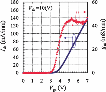 DC characterization (Figure 2) showed a threshold voltage of +3V and maximum drain current (Ids(max) of 138mA/mm at a gate potential (Vgs) of +7V. The maximum transconductance of 45mS/mm occurred at Vgs of +5V. The researchers attribute the high positive threshold to the use of non-polar m-plane GaN, Al2O3 dielectric, and a recessed gate.
Figure 2: Transfer characteristics at a source–drain voltage of 10V for UCSB/Rohm E-mode m-plane AlGaN/GaN HFETs.
The sub-threshold performance was assessed at a source–drain potential (Vd) of 10V. The device is described as being completely off at Vgs of 0V with a leakage current (Ioff) of 3.46x10⁻⁸A/mm. The on/off ratio (Ids(max)/Ioff) is thus 4x10⁶. The researchers say that this value is higher than that reported for other E-mode m-plane AlGaN/GaN HFETs. The on/off ratio is attributed to the use of m-polar GaN, the high dielectric constant of Al2O3, and a low interface trap density.
The UCSB/Rohm researchers say that no data had been previously presented on the interface properties of Al2O3 and m-plane nitride semiconductor material. Therefore, the team first carried out photo-assisted capacitance–voltage (C–V) measurements to assess the quality of the Al2O3 interface with m-plane GaN.
MOCVD was used to create 1μm of unintentionally doped GaN, 0.5μm 3x10¹⁸/cm3 silicon-doped n-GaN, and 0.3μm 3x10¹⁷/cm3 silicon-doped n-GaN.
The Al2O3 ALD (in both the interface characterization and in the final HFET) was preceded by a hydrochloric acid treatment at room temperature. The 20nm Al2O3 layer was deposited in two stages: 2nm at 200mTorr and then 18nm at 20mTorr. The higher-pressure step (with hydrogen/argon carrier) has been found to reduce the subthreshold slope properties of the structure from 270mV/decade to 170mV/decade. The lower pressure deposition used a pure argon carrier.
The sample was annealed at 400°C in 10%/90% hydrogen/nitrogen forming gas. A titanium-gold contact was used on the Al2O3 and an aluminum-gold contact was recessed into the n-GaN layers.
The density of traps between 0.2eV and 0.6eV from the conduction is estimated at 1–2x10¹²/cm2-eV. The researchers comment: “This value is almost comparable with reported values of Al2O3/c-plane GaN”.
There is a peak of 5x10¹²/cm2-eV around 0.9eV that is attributed to holes that can be generated by the ultraviolet (UV) radiation used in the C–V measurements. The UV light source had wavelength peaks at 365nm, 405nm, and 436nm. These peaks are the i-, h- and g-lines, respectively, of the mercury emission spectrum.
Financial and other support for the work came from UCSB’s Solid State Lighting and Energy Center, US Office of Naval Research (ONR), DRIFT, and the UCSB nanofabrication facility (which is part of the US National Nanotechnology Infrastructure Network).
Polarization junctions increase nitride transistor breakdown voltage
AlGaN/GaN HFETs HEMTs GaN GaN substrates MOCVD ALD
The author Mike Cooke is a freelance technology journalist who has worked in the semiconductor and advanced technology sectors since 1997.