- News
25 August 2011
First noise assessment of AlN/GaN HEMTs on silicon
France’s Institute of Electronic, Microelectronic and Nanotechnology (IEMN) has given the first evaluation of the noise performance of its aluminum nitride/gallium nitride (AlN/GaN) on silicon high electron mobility transistors (HEMTs) [F. Medjdoub et al, IEEE Electron Device Letters, published online 8 August 2011].
IEMN reported its novel approach to producing higher performing nitride HEMTs on low cost silicon substrates a couple of months ago (for further details see Semiconductor Today reports in June 2011, for example, Combining high current with high transconductance).
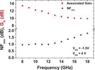
 In the new work, the noise performance was tested between 8GHz and 18GHz (Figure 1). At the optimum bias (drain-source, VDS, of 4V and gate-source, VGS, of -1.5V), the minimum noise figure (NFmin) was around 1dB with associated gain (GA) of more than 11dB up to 12GHz. At 18GHz, NFmin was 1.8dB and GA 10dB. The researchers comment: “These data are comparable to the best reported GaN-on-Si HEMT values.” The occurrence of the minimum noise figure under the same bias conditions as the maximum associated gain is “highly favorable for circuit designs”.
Figure 1: Associated gain and minimum-noise figure as function of frequency biased at VGS of 1.5V and VDS of 4V at room temperature.
The equivalent noise resistance was 45-41Ω in the range 8-18GHz, “even lower than the state-of-the-art 0.1μm GaN-on-Si HEMTs and indicates an excellent potential for broadband low-noise amplifiers.”
This performance is achieved despite the higher self-heating effects that are due to the lower thermal conductivity of silicon compared with silicon carbide (SiC) substrates. Also, SiC has a smaller mismatch in lattice parameter than Si for growth of GaN. Lattice mismatch creates defects that can lead to parasitic electrical conduction at the substrate buffer interface.
The researchers attribute its results to the high transconductance and the low gate leakage current found in its AlN/GaN/Si devices. They comment: “In addition, further improvement of the fairly high contact resistances and the reduction of the gate length should definitely enable sub-1dB microwave noise performance.” IEMN thus sees AlN/GaN HEMTs as being “an excellent candidate for the next generation of millimeter wave monolithically integrated circuits”.
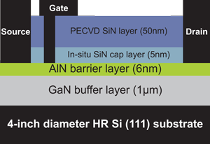
 High resistive silicon was used as substrate (5000Ω-cm, 4-inch wafer). The devices layers, up to and including the in situ silicon nitride (Figure 2), were grown with metal-organic chemical vapor deposition by EpiGaN. The titanium-aluminum-nickel-gold ohmic contacts were formed by etching down to the AlN barrier layer. The contacts were annealed in an 850°C rapid thermal process in nitrogen. Nitrogen ion implantation was used to isolate devices. Plasma-enhanced chemical vapor deposition of silicon nitride was then performed.
Figure 2: Schematic cross-section of fabricated AlN/GaN-on-Si HEMTs.
The nickel-gold gate was formed by electron-beam lithography and etching through the SiN with sulfur hexafluoride plasma. A field-plate extension of 0.2μm toward the drain was used to modify the electric field in the device. The gate length was 0.16μm. The gate-source and gate-drain distances were 0.3μm and 1μm, respectively. The device width was 50μm (2x25μm).
The maximum current density at 2V gate potential was 1.97A/mm. The gate leakage was less than 100μA up to 80V reverse bias. This low value is attributed to the high barrier provided by the use of high quality AlN and the presence of the in situ SiN cap that gives a robust surface, avoiding gate tunneling at high field. The 1mA/mm gate-drain breakdown voltage is more than 100V.
The extrinsic transconductance peaks at 606mS/mm with the source-drain potential at 4V and the source-gate at -1.5V. This high value is credited on the short gate-channel distance and the high drain current density.
Extrapolation of the S-parameters at optimum bias measured between 1GHz and 50GHz give current gain extrinsic cut-off (fT) and maximum oscillation (fmax) frequencies of 85GHz and 103GHz, respectively. The field plate impacts the fmax value by increasing the gate-drain capacitance. The cut-off gate-length product (fTxLg) value of 13.6GHz-μm gives hope of very high frequency operation with downscaling. The high current density and breakdown voltage should also enable the researchers to access high output power performance.
Combining high current with high transconductance
Record transconductance for nitride HEMT on silicon
AlN barrier increases output current from GaN/Si HEMTs
The author Mike Cooke is a freelance technology journalist who has worked in the semiconductor and advanced technology sectors since 1997.