- News
8 August 2011
InGaN/GaN DHBTs achieve cut-off of more than 5GHz
Georgia Institute of Technology has reported n-p-n indium gallium nitride/gallium nitride (InGaN/GaN) double-heterostructure bipolar transistors (DHBT) with relatively high collector current and frequency performance [Shyh-Chiang Shen et al, IEEE Electron Device Letters, vol32, p1065 August 2011]. The researchers comment on their work: “To the best of our knowledge, this letter is the first RF demonstration of GaN/InGaN HBTs with fT > 5GHz.”
While nitride semiconductor high-electron-mobility field-effect transistors (HEMTs) have achieved kiloVolt breakdown voltages and cut-off frequencies of more than 200GHz, III-nitride bipolar transistors have shown less useful performance. Some progress has been made in producing reasonable DC characteristics such as high voltage, current gain and temperature performance in various n-p-n heterostructure transistor (HBT) and DHBT systems, for example, aluminum gallium nitride/gallium nitride (AlGaN/GaN), InGaN/GaN or pure GaN.
However, results published so far show particular weakness in terms of frequency and collector current performance. In efforts to improve this, the Georgia Tech researchers used techniques previously developed by some of themselves to reduce dislocation and V-defects in graded InGaN DH structures. In particular, a graded base–emitter junction was used to avoid V-defects. A graded base–collector junction was designed to eliminate the conduction band discontinuity between InGaN and GaN.
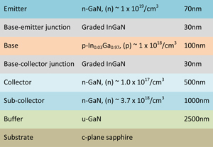 Figure 1. Epitaxial layer structure for DHBT.
The InGaN DHBT structures (Figure 1) were grown on c-plane sapphire substrates using metal-organic chemical vapor deposition (MOCVD). A three-step mesa was etched with inductively coupled plasma (ICP) consisting of chlorine/helium to create emitter, base and isolation structures. Etch-induced surface damage was removed using dilute potassium hydroxide (KOH)/potassium persulfate (K2S2O8) solution under ultraviolet illumination.
The base contact consisted of nickel-gold, while the emitter and collector contacts were titanium-aluminum-titanium-platinum and titanium-aluminum-titanium-gold, respectively. Benzocyclobutene (BCB) was used for passivation. To access the emitter, base and collector contacts, holes were etched in the BCB using ICP. Device interconnects and RF probe pads consisted of titanium-gold (Figure 2).
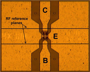 Figure 2. Microscope picture of fabricated GaN/InGaN DHBT with emitter area 4μm x 10μm. The device is designed in common-emitter ground–signal–ground (G–S–G) coplanar waveguide (CPW) configuration for RF measurement.
Common-emitter DC characteristics of the 3μm x 5μm emitter area device include a collector current of 2.4mA (16kA/cm2) at a base current of 100μA, giving a current gain of 24. The open base breakdown voltage was 95V at 1μA collector current.
RF measurements were performed on a 4μm x 20μm emitter device, giving a 20dB extrapolation for the cut-off frequency (fT) of 5.3GHz, at collector current density of 4.7kA/cm2 and collector–emitter voltage of 7V. Further study of the RF performance showed deviation from the usual 20dB fall-off at high frequency, partly due, it is thought, to capacitive coupling between emitter and collector.
The researchers comment: “This parasitic component comes from the extensive overlay of the emitter ground-plane metal and the underlying thick (2500nm) unintentionally doped (n ~ 1016/cm3) GaN buffer layer that electrically connects to the subcollector in the common–emitter CPW design”
The parameter (Mason’s unilateral gain, U) used to determine a maximum oscillation frequency (fmax) of 1.3GHz also did not roll-off at the standard 20dB/dec, “because the curve is still transitioning from the low-frequency gain region to the high-frequency roll-off region before it reaches the unit-gain frequency”.
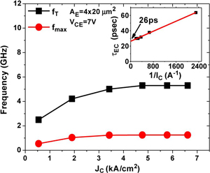 Figure 3. fT and fmax of GaN/InGaN DHBT with emitter area 4μm x 20μm at different collector current densities (JC).
The dependences of the cut-off/maximum oscillation frequencies on collector current were also explored (Figure 3). The values trend up with current, saturating after densities of around 5kA/cm2 and 3kA/cm2, respectively. The emitter–collector transit time (τEC) was derived from 1/(2πxfT). The devices could only be run up to 7kA/cm2 due to thermal runaway effects and catastrophic damage at higher current.
The researchers say that possible RF performance improvements for GaN/InGaN HBTs could include further reduction in the base resistance and growing these structures on substrates with better thermal conductivity to achieve higher current operation. Sapphire is a poor base for devices that need to dissipate generated heat due to its very low thermal conductivity compared with silicon carbide, GaN, or even silicon.
http://dx.doi.org/10.1109/LED.2011.2156378
The author Mike Cooke is a freelance technology journalist who has worked in the semiconductor and advanced technology sectors since 1997.