- News
19 April 2011
Re-grown source–drain III-V MOSFETs demonstrate higher drain current
Tokyo Institute of Technology has increased the maximum drain current of indium gallium arsenide (InGaAs) complementary metal–oxide–semiconductor (CMOS) field-effect transistors (FETs) to more than 1.3mA/μm [Ryousuke Terao et al, Appl. Phys. Express, vol4, p054201, 2011].
Researchers have been working to achieve saturation drain currents of 2mA/μm for future scaled CMOS devices and moving from silicon to high-mobility III-V channels such as InGaAs has been developed as an option to achieve this. Earlier this year, a Taiwan National Tsing Hua University/National Taiwan University group reported a drain current of 1.23mA/μm – “to our knowledge, the present maximum drain current”, the Tokyo researchers comment.
The Tokyo researchers achieved their improved drain current by increasing the carrier concentration in the source–drain regions through using metal-organic chemical vapor deposition (MOCVD) re-growth rather than ion implantation to create highly silicon-doped InGaAs. The maximum carrier concentrations of ion-implanted InGaAs is about 1019/cm3. Using re-growth, this can be increased about 3x.
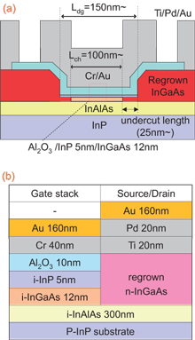 The epitaxial layers for the latest Tokyo device (Figure 1) were grown on p-type indium phosphide (InP) substrates using MOCVD. The InGaAs channel layer was not doped (intrinsic/i-) to avoid resistance effects arising from ionized impurity scattering. The channel was covered with a thin 5nm i-InP layer to separate the carrier distribution from the oxide interface, avoiding further resistance effects from interface roughness and charge traps. The 300nm i-InAlAs layer below the channel further confined the channel carrier distribution.
Figure 1: (a) Schematic and (b) layer profile at the gate stack and source/drain structure of the fabricated re-grown source/drain MOSFET.
A ‘dummy gate’ structure consisting of silicon dioxide was then formed on the top InP layer with lengths in the range 150nm to 6μm, with a channel width of 20μm. The purpose of the dummy gate was to allow wet etch of the InP and InGaAs layers in the source–drain regions, using hydrochloric acid in water and citric acid in hydrogen peroxide, respectively. The InGaAs etch also undercut the dummy gate on both sides — about 25nm for deep submicron channels (thus 150nm dummy gate gives 100nm channel) and 45nm for micron-scale channels.
The wet etch was followed by an InAlAs surface treatment with a more dilute hydrochloric acid solution (1:5 rather than 3:1).
The source–drain regions were then formed from silicon-doped InGaAs regrown using MOCVD. A dummy sample of regrown n-InGaAs on InAlAs/semi-insulating InP was found to have a carrier concentration of 2.9x10¹⁹/cm3 and a mobility of 1490cm2/V-s. The researchers comment: “Thus, the re-grown source/drain process seems to be a good technique for heavy doping”.
The devices were then isolated and the dummy gate was removed using buffered hydrofluoric acid. Atomic layer deposition (ALD) was used to apply aluminum oxide (Al2O3) gate insulator/dielectric. The wafer was then annealed at 400°C in nitrogen.
The gate electrode metals were then formed and annealed (350°C in nitrogen), followed by etch of the Al2O3 and deposition of the source–drain metal.
For the shortest channel length of 100nm, the maximum drain current of 1.34mA/μm was obtained with drain bias 1V and gate potential 3V. The gate leakage under these bias conditions was 2.6x10⁻⁶mA/micron, a factor of more than 105 smaller than the drain current. The peak transconductance of 817microS/μm was obtained at drain bias 0.65V. The threshold was –0.3V, so the device is partially ‘on’ at 0V (depletion mode, normally-on).
The total series resistance of the MOSFET was 0.5kΩ-μm, “which is slightly worse than other reported values”, the researchers comment. The poor series resistance is thought to arise from “high contact resistance of the metal/semiconductor junction”. From transmission line method (TLM) measurements, the researchers estimate that 0.38kΩ-μm of the total series resistance arose from contact resistance, with the remainder being due to sheet resistance. Subtracting the series resistance gave an intrinsic transconductance figure of 1330microS/μm. The researchers thus hoped for improved performance from improving the metal/semiconductor contact properties.
The estimated peak channel mobility was 3100cm2/V-s. The substhreshold swing at a drain voltage of 10mV was 184mV/dec and at 0.65V it was195mV/dec. While these are a way off from the theoretical limit of 60mV/dec of planar MOSFET structures, the researchers comment: “This value is a dramatic improvement compared with our previous device (nearly 1 V/decade)”. One possible reason for the improvement is thought to be a reduction in the dielectric/semiconductor interface trap density as a result of surface cleaning, sulfide treatment, trimethyl-aluminum (TMA) pretreatments, and annealing before the Al2O3 gate dielectric deposition.
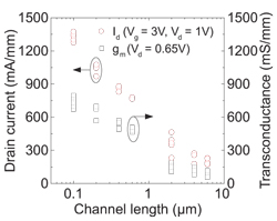 Comparing the performance of devices with different channel lengths (Figure 2), the researchers note “a good trend of increasing output performance with scaling of the channel length, although we also have room to improve the characteristics by using thinner Al2O3”. There was some degradation of drain current and threshold fluctuation that seem to be associated with charge trapping; further work is needed to analyze and suppress these effects.
Figure 2: Channel length dependence of drain current (Id) at drain bias (Vd) 1V and gate potential (Vg) 3V, and peak transconductance (gm) at Vd 0.65V.
The researchers conclude that their results “indicate that the [metal-organic vapor phase epitaxy] MOVPE [i.e. MOCVD] re-growth process has superior capabilities for high-current operation”.
Self-aligned Ni-InGaAs as source–drain for InGaAs MOSFET
Power, speed and other highlights of IEDM 2010
Capacity of InGaAs to increase drive current in nano MOSFETs
The author Mike Cooke is a freelance technology journalist who has worked in the semiconductor and advanced technology sectors since 1997.
Join Semiconductor Today's LinkedIn networking and discussion group