- News
25 April 2011
Sapphire patterning boosts green light generation and extraction
Researchers from Rensselaer Polytechnic Institute (RPI) in the USA and SCIVAX Corp of Japan have used patterned sapphire substrates to improve efficiency of green (520–570nm wavelength) light-emitting diode (LED) indium gallium nitride (InGaN) semiconductor structures [Yufeng Li et al, Appl. Phys. Lett., vol98, p151102, 2011].
Patterning of sapphire substrates has previously been used to reduce total internal reflection of light (due to refractive index differences of materials) back into nitride semiconductor devices, increasing light extraction. However, another effect of patterning can also be to improve the crystal quality of epitaxial nitride semiconductor layers. One way to do this is to deposit a silicon dioxide mask to block threading dislocations and create regions of low-defect material (epitaxial layer overgrowth/ELOG).
Direct patterning of sapphire substrates has also been suggested as a way to reduce threading dislocations in epitaxial layers, and was recently used by researchers based in Taiwan to enhance the performance of nitride semiconductor photovoltaic devices [Improving PV material quality with patterned sapphire].
The RPI/SCIVAX researchers used nano-imprint lithography (NIL) with a silicon patterned stamp to produce patterning in a resin layer on the initially planar sapphire substrates. Reactive ion etch (RIE) then transferred the patterning of the resin layer, cutting into the sapphire itself to create a hexagonal array of cylindrical holes of 250nm diameter and 450nm period. The etch depth was 125nm.
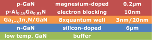
Figure 1 (above): Schematic of epitaxial nitride layers grown on patterned and unpatterned sapphire substrates. The grown devices had In content of 10–20%, determined through x-ray diffraction.
 Vertical-flow metal-organic chemical vapor deposition (MOCVD) was used to grow the nitride semiconductor layers on these patterned sapphire substrates (Figure 1). Patterning was found to improve the crystal quality of the nitride semiconductor material through reducing threading dislocation (TDs) densities (Figure 2) in the quantum wells of the LEDs where the light is produced.
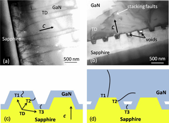
Figure 2 (right): Cross-section TEM of the epitaxial GaN/sapphire interface on planar (a) and nanopatterned (b) sapphire. Schematics showing early (c) and late (d)
phases of threading dislocation
(T1, T2, T3) formation on nanopatterned substrates.
Threading dislocations emanating from the bottom of the cylinders (T3) are thought to be terminated by air voids that tend to form during the growth process. Another TD reduction process is thought to be confinement to the growth plane of those emanating from the cylinder sidewalls (T2). “Only TDs originating in the un-etched portions of the substrate (T1) propagate toward the active region,” the researchers comment.
The researchers estimate from transmission electron microscopy (TEM) that the threading dislocation density is 3.6x10⁸/cm2 for patterned substrate growth, reduced 44% compared with 6.4x10⁸/cm2 for the unpatterned substrates. X-ray diffraction (XRD) linewidths were also reduced to 427arcsec from 524arcsec, again suggesting improved crystal quality for the patterned over the unpatterned material, respectively.
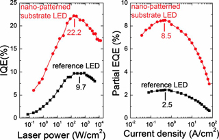 The internal quantum efficiency (IQE) was estimated using photoluminescence (PL) at both 7K and room temperature with excitation from a laser at 408nm (so the non-active layers are not excited). The maximum IQE for the patterned material was 22%, while the unpatterned reference only managed 9.7% (Figure 3a). This gives the patterned material an advantage of more than 2x.
Figure 3: (a) IQE as a function of excitation power density, (b) EQE as a function of current density for nanopatterned substrate (circles) and reference (squares) LED.
Electroluminescence tests (Table 1) on 350μm x 350μm LEDs (without encapsulation) provided further information on external quantum efficiency (EQE) through the substrate side (Figure 3b) and thus the light extraction efficiency (LEE). The maximum EQE was 8.5% at 0.5A/cm2 for the patterned device, which is a 3.4x advantage compared with the 2.5% at 0.8A/cm2 achieved for the reference.
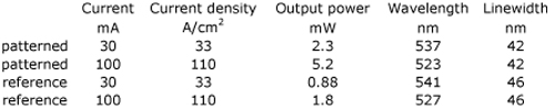
Table 1: LED characteristics for devices grown on patterned and unpatterned sapphire (reference). Output power is partial, being measured from the sapphire side of the unencapsulated nanopatterned substrate LED die.
By studying the angular distribution of the light output power and interference effects, the researchers estimate an LEE enhancement of 1.58x from the reduction of total internal reflection of light due to the patterning.
Taking the a-plane to higher crystal quality
Osram doubles green LED brightness for 2-meter office projectors
UCSB uses more uniform InGaN for record efficiency semi-polar green LED
RPI Green LEDs InGaN Patterned sapphire substrates MOCVD
The author Mike Cooke is a freelance technology journalist who has worked in the semiconductor and advanced technology sectors since 1997.