- News
1 April 2011
Towards CMOS-compatible HEMTs
Massachusetts Institute of Technology (MIT) has developed gold-free ohmic contacts for nitride semiconductor high-electron-mobility transistors on silicon substrates with performance close to that of traditional contacts containing gold [Hyung-Seok Lee et al, IEEE Electron Device Letters, published online 20 March 2011].
Since the development of gallium nitride layers on silicon, researchers have considered the possibility of developing integrated devices combining the high-frequency/power/temperature capabilities of nitride semiconductors with the logic versatility of high-performance silicon electronics. A particular attraction is the commercial availability of six-inch (150mm) gallium nitride on silicon wafers that could be used in fabrication facilities originally designed for silicon devices such as silicon-based power transistors.
One hurdle to overcome in this is the use of gold in producing ohmic connections to the source and drain regions of nitride field-effect transistors. The problem is that gold is not allowed in silicon device fabrication, since gold produces acceptor and donor levels in silicon that poison device performance.
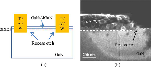
Figure 1: (a) Schematic cross section of the fabricated undoped AlGaN/GaN HEMTs with S/D ohmic recess. (b) SEM image of the cross section of a Ti/Al/W contact after annealing. Before metallization, the ohmic contact region was recessed ~30nm.
The presence of gold in the typical ohmic metal layer stack titanium/aluminum/XY/gold (Ti/Al/XY/Au) is thought to improve the contact resistance by creating gallium vacancies in the nitride semiconductor material and by preventing oxidation of the stack by the atmosphere. The XY-layer is a diffusion layer (typically nickel, palladium or molybdenum). On the negative side, long-term gold diffusion has also been associated with degradation of the ohmic contacts. This latter possible effect gives another motivation for developing gold-free set-ups.
Selective doping of the source–drain contacts has been attempted in creating gold-free processes, but these methods tend to reduce breakdown voltages and increase leakage currents. Complicated re-growth methods have also been attempted — however, these would be expensive to implement in manufacturing.
The MIT researchers used 4-inch (111)-oriented silicon wafers (100mm diameter) on which nitride semiconductor layers had been grown using metal-organic chemical vapor deposition (MOCVD): the undoped GaN buffer layer was 1.8μm thick; the AlGaN (26% Al) barrier and undoped GaN cap layers were 17.5nm and 2nm, respectively.
The mesa isolation and recessing were carried out using electron cyclotron resonance (ECR) etching with boron trichloride/chlorine plasma. The metal contact stack was deposited using electron-beam evaporation. The gold-free stack consisted of titanium (Ti), aluminum and tungsten (W). The final tungsten layer forms a barrier to prevent oxidation of the aluminum.
Rapid thermal annealing was used with a temperature of 600–1000°C. It was found that annealing at more than 800°C (900°C for samples without recess) was needed to give linear ohmic behavior.
Various recessing depths were tried: 0nm (i.e. no recessing), 15nm and 30nm. A gold-based stack (titanium-aluminum-nickel-gold) was also produced as a control sample. The lowest contact resistance for the gold-free set up was obtained with 30nm recessing: 0.49Ω-mm with 870°C anneal. The best results for no recessing and 15nm recessing were 2.02Ω-mm (950°C anneal) and 1.71Ω-mm (870°C), respectively. The anneal times for these results were 30 seconds.
The full recessing of 30nm puts the ohmic metal stack in contact with the two-dimensional electron gas (2DEG) that forms the channel of the nitride semiconductor HEMT. It is also thought that formation of nitrided Al and Ti after annealing reduces the energy barrier between the contact metal and 2DEG.
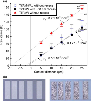 Specific contact resistances were measured using linear transmission line method (LTLM) structures (Figure 2). The Ti/Al/W stacks with (30nm) and without recessing had specific contact resistances of 6.5x10⁻⁶Ω-cm2 and 8.7x10⁻⁵Ω-cm2, respectively. The value for the control Ti/Al/Ni/Au contact annealed at 870°C was 3.1x10⁻⁶Ω-cm2. The contact resistance for the control was 0.38Ω-mm.
Figure 2: (a) Total resistance for different ohmic metallization processes as function of contact distance. (b) Optical micrograph images of the surface for (left) Ti/Al/W recessed contacts and (right) standard Ti/Al/Ni/Au contacts.
The researchers also studied the surface smoothness (Figure 2b) of the various contacts (morphology). The gold-free contact (Ti/Al/W) was much smoother, due, it is thought, to the absence of AuAl4 alloys. Such smoothness is an advantage in highly scaled (i.e. ultra-small) devices.
Apart from the source–drain ohmic contact structures, all samples underwent nominally the same epitaxial and fabrication processes.
After the source–drain contacts had been formed, the gate structure (3nm Ga2O3 dielectric, Ti/Al/W metal electrode stack) was formed and 20nm Al2O3 passivation was applied with atomic layer deposition. The Ga2O3 dielectric was formed by exposing the gate region to oxygen plasma.
The produced transistors had gate lengths of 3μm. The gate–source and gate–drain distances were both 1.5μm. All the devices had a threshold voltage of about –2.2V (depletion-mode, normally-on), gate leakage less than 10mA/mm, and 87V three-terminal breakdown (at gate potential of –6V).
However, the 100mA/mm on-current behavior was much improved through recessing with a source–drain voltage drop of only 0.78V, rather than the 1.31V needed for the non-recessed sample. The traditional gold-based contacts had a 0.68V drop at the same current level. The recessed contacts therefore have only a 15% increased voltage compared with the traditional control structure. Since the devices are ‘normally-on’, the gate potential in these measurements is zero.
The researchers conclude: “These results enable the fabrication of high-performance GaN power devices in Si fabs without the risk of contaminating the Si wafers, which enables the large-scale production of GaN power electronics.”
The MIT research was financially supported in part by the US Advanced Research Projects Agency—Energy (ARPA-E) Agile Delivery of Electrical Power Technology (ADEPT) program.
http://dx.doi.org/10.1109/LED.2011.2114322
The author Mike Cooke is a freelance technology journalist who has worked in the semiconductor and advanced technology sectors since 1997.
Join Semiconductor Today's LinkedIn networking and discussion group