| Home | About Us | Contribute | Bookstore | Advertising | Subscribe for Free NOW! |
| News Archive | Features | Events | Recruitment | Directory |
News
18 October 2010
Advancing infrared emission from nitride LEDs
Researchers based in the USA have used erbium (Er) doping to create nitride infrared (IR) light-emitting diodes (LEDs) with dominant emission under forward bias [R. Dahal et al, Appl. Phys. Lett., vol97, p141109, 2010].
Although the output power of 2μW at an injection current of 20mA might appear very low compared with the tens of milliwatts performance of blue-ultraviolet nitride LEDs, the researchers at Texas Tech University, Kansas State University, and Polytechnic Institute of New York University believe their IR LEDs ‘represent a significant advance in the development of current-injected, chip-scale emitters and waveguide amplifiers based on Er-doped semiconductors.’
Normally, nitride LEDs emit in the range from green to deep ultraviolet (530–200nm). Some research groups have attempted to produce devices with longer wavelengths by doping the nitride material with rare-earth elements such as Er and europium (Eu) with a view to infrared optical communications and full-color display systems.
Erbium has 4f transitions that fall in the 1.5μm minimal loss window of optical fiber technology. Wide-bandgap nitride semiconductors doped with Er have an excitation cross-section (~10-15cm2) that is up to five orders of magnitude better than that of conventional erbium-doped fiber amplifiers (~10-20cm2). This raises the hope that Er-doped nitride semiconductors could achieve room-temperature operation of electrically pumped emitters and amplifiers operating at 1.54μm.
Previous Er-doped nitride devices have been created using ion implantation or in-situ doping in molecular beam epitaxy (MBE) systems. These devices emitted more light under reverse bias conditions (up to several hundred volts), suggesting impact energy transfer as the excitation mechanism in these cases.
The researchers prefer to use the more commercial production growth process of metal-organic chemical vapor deposition (MOCVD). Previously, they deposited Er-doped gallium nitride (GaN) and indium gallium nitride (InGaN) epilayers on commercially available III-nitride UV/blue LED wafers. This gave low-efficiency devices, since the Er excitation was through optical pumping from light emitted from the blue LED layers.
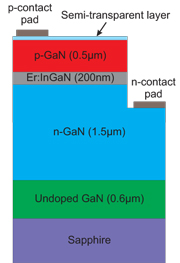 Figure 1: Multilayer structure of the p-GaN/Er:InGaN/n-GaN LEDs. Active region is a 200nm-thick Er-doped In0.05Ga0.95N epilayer.
The new devices have an Er-doped intrinsic nitride layer sandwiched between p-type and and n-type layers in a p-i-n format (Figure 1). MOCVD was used to create the diode structure on a (0001) sapphire substrate. The n- and p-type dopings were achieved using silicon and magnesium, respectively. These achieved carrier concentrations of 5x10¹⁸/cm3 and 3x10¹⁷/cm2. The corresponding mobilities were 250cm2/V-s and 10cm2/V-s. An annealing step raising the temperature to 550°C for 30min in nitrogen was used to activate the magnesium doping. The ‘intrinsic’ In0.05Ga0.95N layer had an erbium doping concentration ~2x10¹⁹/cm3.
The LEDs were created from 300μm x 300μm mesas with a semi-transparent nickel-gold p-contact and a titanium-aluminum-titanium-gold n-contact. Electrical characterization of the device showed a low leakage current of 0.2μA at a reverse bias of –15V. However, a high forward voltage of 12.5V is needed for a 20mA forward current.
This high forward voltage is significantly higher than those usually observed in multi-quantum well nitride LEDs (3–4V). The researchers comment that the Er-doped i-layer is not optimized for conductivity. They comment: “The forward voltage can be reduced by optimizing the active layer thickness and by employing Si co-doping. However, there could be trade-offs among the active layer thickness, Si co-doping concentration and EL intensity, which will require further investigations.”
The main emissions under electroluminescence (Figure 2) are peaks at green wavelengths of 536nmand 556nm, a red wavelength of 667nm, and near-infrared emissions of 1μm and 1.54μm. The visible peaks were not seen in photoluminescence experiments. The researchers associate the emissions with various transitions between 4f levels of the Er electronic levels.
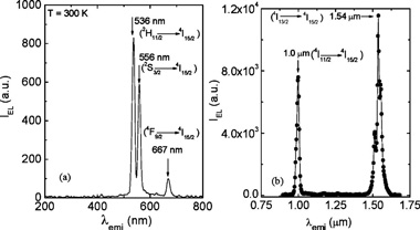
Figure 2: Room-temperature electroluminescence spectra of Er-doped nitride LED (a) in visible region, and (b) in near-IR region under 20mA current injection with a forward bias of 12.5V.
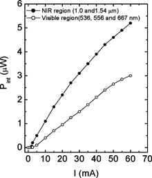 Integrated power measurements were also made (Figure 3). The infrared emission (~2μW) was about twice that of the visible (~1μW) at 20mA. These values are comparable with those of other groups using red-emitting europium-doped nitride LED structures. More detailed study of the infrared emission shows that the 1.54μm line dominates for currents less than 30mA, while the 1.0μm line becomes the stronger for higher currents.
Figure 3: Integrated optical power, over the visible and near IR regions, of Er-doped nitride LED as a function of input forward current.
The researchers comment: “These results are very promising for development of Er-doped 1.54μm emitters having very stable RT operation. They also present an important step in the development of current-injected chip-scale optical amplifiers active in the 1.54μm wavelength window for future optical communication applications.”
![]() Search: IR LEDs MOCVD GaN InGaN
Search: IR LEDs MOCVD GaN InGaN
Visit: http://link.aip.org
For more: Latest issue of Semiconductor Today
The author Mike Cooke is a freelance technology journalist who has worked in the semiconductor and advanced technology sectors since 1997.
![]() ©2010 Juno Publishing and Media Solutions Ltd. All rights reserved. Semiconductor Today and the editorial material contained within it and related media is the copyright of Juno Publishing and Media Solutions Ltd. Reproduction in whole or part without permission from Juno Publishing and Media Solutions Ltd is forbidden. In most cases, permission will be granted, if the author, magazine and publisher are acknowledged.
©2010 Juno Publishing and Media Solutions Ltd. All rights reserved. Semiconductor Today and the editorial material contained within it and related media is the copyright of Juno Publishing and Media Solutions Ltd. Reproduction in whole or part without permission from Juno Publishing and Media Solutions Ltd is forbidden. In most cases, permission will be granted, if the author, magazine and publisher are acknowledged.
Disclaimer: Material published within Semiconductor Today and related media does not necessarily reflect the views of the publisher or staff. Juno Publishing and Media Solutions Ltd and its staff accept no responsibility for opinions expressed, editorial errors and damage/injury to property or persons as a result of material published.
Semiconductor Today, Juno Publishing and Media Solutions Ltd, Suite no. 133, 20 Winchcombe Street, Cheltenham, GL52 2LY, UK
Web site by No Name No Slogan ![]()