- News
30 November 2010
Putting on a bow-tie for higher-energy nitride laser performance
Japan’s Sony Corp and Tohoku University’s New Industry Creation Hatchery Center (NICHe) have added bow-tie waveguide structures to increase the energy output of nitride semiconductor self-pulsating laser diodes (SP-LDs) to 310 picoJoules/pulse (pJ/pulse) [Hideki Watanabe et al, Appl. Phys. Express, vol3, p122103, 2010]
The researchers are seeking laser diode technology that can meet the needs of next-generation volumetric (i.e. three-dimensional rather than two-dimensional) optical storage based on multi-photon absorption. Memory media for such technology has already been developed, but operation at present needs large, expensive solid-state lasers, such as those using titanium-doped sapphire, which are only found in research laboratories.
The Sony–NICHe group has previously succeeded in operating volumetric optical storage using a laser system consisting of two parts: a mode-locked gallium nitride (GaN) laser diode and a semiconductor optical amplifier (SOA) to generate 100W peak power. High power is needed to achieve the multi-photon absorption process that is required to create the changes in the storage medium. Also, a short wavelength is desired to increase storage densities.
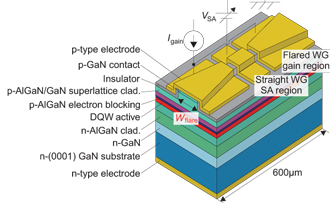 Rather than using multi-stage systems, a single laser diode that provides the necessary energy is sought. With this in mind, the Sony–NICHe group has a developed a self-pulsating laser diode (SP-LD) with a bow-tie ridge waveguide (WG) structure (Figure 1). The hope was to boost output powers over SP-LDs with straight WGs (<10W). The ‘bow-tie’ reduces field densities in the output facet regions, suppressing gain saturation and catastrophic optical damage (a common cause of laser diode failure).
Figure 1: Structure of GaN-based bow-tie SP-LD.
The Sony–NICHe group has previously produced a non-tapered SP-LD structure with 10W peak power and pulses of energy 150pJ. Using the bow-tie structure, this has been increased to 20W peak and 310pJ/pulse. A previous record (1994) for bow-tie laser diodes in another material system obtained 7W peak and 100pJ/pulse.
The Sony–NICHe SP-LD was grown on n-GaN using metal-organic chemical vapor deposition (MOCVD). The double quantum well (DQW) active region consisted of Ga0.92In0.08N wells and Ga0.98In0.02N barriers.
The ridge waveguide (WG) structuring was performed using reactive ion etching (RIE). The cavity was 600μm long, and the GaN-based saturable absorber (SA) region had a ridge WG that was 1.5μm wide and 10μm long. The bow-tie flared regions had a width at the two facets of up to 5μm (Wflare). These regions were 292μm long. Laser diodes with 2.5μm Wflare and non-tapered WGs were also produced for comparison purposes.
The p-type ohmic electrode was removed between the gain and the SA to electrically separate these regions. The front and rear facets were coated with Al2O3 and TiO2/Al2O3 dielectric multi-layers, offering reflectivities of 5% and 95%, respectively. The laser diode chip was put in a 5.6mm-diameter can and, during testing, was kept at 25°C using a Peltier cooling system.
Peak operation was obtained with a gain current of 550mA and an SA reverse-bias of –10V. The optical pulse duration was 15.5ps and the repetition rate was 0.84GHz. The average output power at a lasing wavelength of 406nm was 260mW. Measurement of the near-field pattern at the front facet indicated that a single mode was generated.
Although the results obtained are promising, wider bow-tie structures are expected to make it difficult to maintain a single tranverse mode, control of which needs further investigation.
The author Mike Cooke is a freelance technology journalist who has worked in the semiconductor and advanced technology sectors since 1997.