| Home | About Us | Contribute | Bookstore | Advertising | Subscribe for Free NOW! |
| News Archive | Features | Events | Recruitment | Directory |
News
9 November 2010
M/A-COM Tech’s Santa Clara Design Center expands to new facility
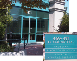
M/A-COM Technology Solutions Inc of Lowell, MA, USA (which supplies semiconductors, components, and subassemblies for RF, microwave and millimeter-wave applications) says that its Santa Clara Design Center has moved to a new facility (near San Jose International Airport and across the street from Santa Clara University) to accommodate its expanded engineering and business functions.
 The design center is focused on the design and development of monolithic pseudomorphic high-electron-mobility transistors (pHEMT) integrated solutions covering 6–50GHz for commercial and military applications. M/A-COM Tech previously announced in May that Henrik Morkner had joined it as director of engineering to lead the team in Santa Clara, and the firm says that the expansion demonstrates its commitment to collaborating with its marketing teams and customers to develop devices.
The new design center occupies about 11,600 square feet and includes a 1200 square foot engineering lab for design and test characterization of monolithic microwave integrated circuits (MMICs), surface-mount devices (SMDs) and connectorized modules. In addition to new product development, the center provides engineering design support and product line management for the Component Product Line, which covers a wide variety of catalog and custom applications.
“This move to a new facility with state-of-the-art equipment allows M/A-COM Tech to fully utilize the talented team we have assembled in Santa Clara for new product development,” says VP engineering Mike Murphy. “Under Henrik’s guidance we are able to work closely with our customers to define and develop products which meet their requirements, both from a technical and commercial approach,” he adds.
![]() Search: M/A-COM Technology pHEMT
Search: M/A-COM Technology pHEMT
Visit: www.macomtech.com
For more: Latest issue of Semiconductor Today
![]() ©2010 Juno Publishing and Media Solutions Ltd. All rights reserved. Semiconductor Today and the editorial material contained within it and related media is the copyright of Juno Publishing and Media Solutions Ltd. Reproduction in whole or part without permission from Juno Publishing and Media Solutions Ltd is forbidden. In most cases, permission will be granted, if the author, magazine and publisher are acknowledged.
©2010 Juno Publishing and Media Solutions Ltd. All rights reserved. Semiconductor Today and the editorial material contained within it and related media is the copyright of Juno Publishing and Media Solutions Ltd. Reproduction in whole or part without permission from Juno Publishing and Media Solutions Ltd is forbidden. In most cases, permission will be granted, if the author, magazine and publisher are acknowledged.
Disclaimer: Material published within Semiconductor Today and related media does not necessarily reflect the views of the publisher or staff. Juno Publishing and Media Solutions Ltd and its staff accept no responsibility for opinions expressed, editorial errors and damage/injury to property or persons as a result of material published.
Semiconductor Today, Juno Publishing and Media Solutions Ltd, Suite no. 133, 20 Winchcombe Street, Cheltenham, GL52 2LY, UK
Web site by No Name No Slogan ![]()