- News
17 November 2010
Developing layer transfer for mixing compound with silicon semiconductors
Transistors with high-mobility indium arsenide (InAs) channels have been built on insulating silicon dioxide (SiO2) layers on silicon substrates by using layer transfer techniques [Hyunhyub Ko et al, Nature, vol468, p289, 2010]. The participating institutions were University of California Berkeley, Lawrence Berkeley National Laboratory, Taiwan’s National Tsing Hua University, and University of New Mexico.
InAs transistors with a gate length of 0.5μm built using this technique achieved ‘on’ currents of 1.4mA/μm with source–drain (VDS) and gate (VGS) voltages of 1V. The researchers describe this ‘on’ current value as ‘impressive’. The on/off current ratio was 104.
The researchers believe that similar layer transfer techniques could be used to put other materials on SiO2/Si substrates to give a range of ‘X-on-insulator’ (XOI) devices.
The InAs layers were first grown on gallium antimonide (GaSb) substrates using molecular beam epitaxy (MBE). The InAs was grown on a previous layer of aluminum gallium antimonide (Al0.2Ga0.8Sb), also deposited using MBE.
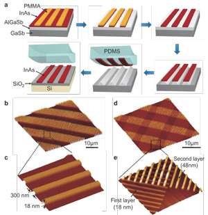 The InAs layer was then transferred to silicon in a number of steps (Figure 1). The InAs is first formed into nano-ribbon strips using lithographic polymethylmethacrylate (PMMA) patterning and citric acid/hydrogen peroxide etching.
The AlGaSb underlayer was then etched using ammonium hydroxide solution to release the InAs nano-ribbons. A 2mm thick polydimethylsiloxane (PDMS) elastomer substrate was used to detach the InAs from the AlGaSb/GaSb and then stamp it onto the SiO2/Si substrate. The SiO2 was thermally grown on the silicon.
The thickness control of the InAs is provided by the epitaxial growth process, while the length and width are determined using lithography. The researchers also experimented with structures where two layers of wires — one 18nm thick and the other 48nm thick — were laid one on top of the other (Figure 1 d, e).
Figure 1: Fabrication scheme for ultra-thin InAs XOI (a), and AFM images (b–e).
The overlay capability is seen as offering capacity for ‘generic heterogeneous and/or hierarchical assembly of crystalline semiconducting materials’, including ‘fabrication of both p- and n-type transistors on the same chip for complementary electronics based on the optimal III–V semiconductors’.
Measurements with atomic force microscopy suggested a surface roughness of less than 1nm. High-resolution transmission electron microscopy (HRTEM) was also used to characterize interfaces between the various materials used.
Two types of transistor were built to test the electronic properties of the InAs material. One construction used the silicon substrate as a back-gate and nickel metal as source/drain contacts to the InAs channel.
A more complex top-gate structure used a zirconium dioxide gate dielectric and nickel gate contact, again with nickel source/drain contacts (Figure 2). Zirconium dioxide (ZrO2) has a high dielectric constant (~20) compared with SiO2’s 3.9. A thermal process at 350°C for 1 minute improved the device performance, creating a 1nm-thick InAsOx passivation layer on the InAs ribbons.
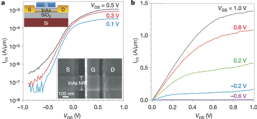
Figure 2: Top-gated InAs XOI FET schematic and transfer (a) and output (b) performance characteristics. The InAs thickness is ~18nm, the ZrO2 is ~8nm. The gate length was 0.5μm (width ~320nm = 0.32μm).
The on/off current ratio for the top-gate device was 104, while the sub-threshold swing (SS=dVGS/d(logIDS)) was 150mV/dec (one device registered 107mV/dec). InAs and InGaAs quantum well FETs have typical SS values of ~70mV/dec and 75mV/dec, respectively. Low values of SS are needed for a sharp switch between ‘off’ and ‘on’. Commercial logic devices have typical SS values of ~70mV/dec. Standard silicon CMOS technology has a fundamental lower limit of 60mV/dec, although alternate channel materials and/or different structures such as tunnel devices could reduce this. The peak transconductance of the InAs transistor was 1.6mS/μm at VDS = 0.5V.
The researchers comment: ‘The devices reported here use a relatively thick gate dielectric, which could be scaled down in the future to further improve the gate electrostatic control and the SS characteristics.’
Using the interface trapping density as a fitting parameter in their device model, the researchers obtained a Dit value of 1011/cm2/eV for the InAsOx passivated device, a 60x improvement over unpassivated transistors. More accurate extraction of Dit using CV (capacitance–voltage) measurements is difficult in narrow-bandgap materials such as InAs compared with silicon-based structures.
The back-gate device was used to study the field-effect mobility for various thicknesses of InAs. For layers less 18nm the mobility increases approximately linearly and then saturates to a value of 5500cm2/V-s. These compared well with simulations performed by the researchers to ‘demonstrate the effectiveness of the XOI platform as a clean and predictable material system for exploring high-performance devices while highlighting the critical role of quantum confinement and surface contributions in the transport properties of InAs, even at relatively large thicknesses’.
The measured saturated field-effect mobility for the back-gate device is around half the comparable figures for InGaAs and InAs quantum well structures of 10,000cm2/V-s and 13,200cm2/V-s, respectively. Field-effect mobilities tend to be lower than bulk values due to device and surface state mobility-reducing contributions that are not present in Hall-effect measurements on bulk material (InAs ~40,000cm2/V-s).
As future research projects, the team is considering using similar layer transfer techniques with other compound semiconductor materials and developing techniques to scale up the process for use with larger-diameter 200mm and even 300mm silicon substrates.
The author Mike Cooke is a freelance technology journalist who has worked in the semiconductor and advanced technology sectors since 1997.