| Home | About Us | Contribute | Bookstore | Advertising | Subscribe for Free NOW! |
| News Archive | Features | Events | Recruitment | Directory |
News
11 November 2010
Top-side TiO2 nanostructures increase blue LED light extraction
Korea University and Chung-Ang University researchers have developed a titanium dioxide (TiO2) nano-structure that boosts light extraction from a blue light-emitting diode (~450nm wavelength) by 12% [Joong-Yeon Cho et al, Jpn. J. Appl. Phys., vol49, p102103, 2010].
Much of the present nitride semiconductor LED research focus is on increasing light extraction efficiency, since the leading LEDs have reached internal quantum efficiencies of 80–90% through continuous improvements in material quality, reducing defects and so on.
However, many of these photons can be trapped by reflections back and absorption in the device structure due to the refractive index difference between gallium nitride (GaN, n ~ 2.5) and air (n ~ 1) or encapsulant (n ~ 1.5).
The external quantum efficiencies of nitride semiconductor LEDs can be increased by reducing reflections at surfaces back into the device using patterning. The blue LEDs in the Korea/Chung-Ang research were grown on sapphire substrates that were patterned for this reason. The new TiO2 structures are designed to reduce reflection at the top-side of the device also.
The TiO2 nanostructured material was deposited on blue GaN LEDs and patterned using nanoimprint lithography (NIL), followed by a lift-off process (Figure 1). The LED had a 120nm indium tin oxide (ITO) transparent conducting layer on the p-GaN injection layer. The researchers constructed the NIL process to avoid the damage to existing structures that can result from many plasma-etch techniques.
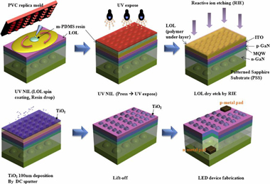
Figure 1: Schematic of overall process flow.
The imprint stamp was made from polyvinyl chloride (PVC) and patterned from a silicon master template in a hot embossing process. The pattern was a periodic series of pillars measuring 300nm diameter at 600nm pitch. The surface of the stamp was covered with 20nm of sputtered silicon dioxide and then coated with a silane-based hydrophobic self-assembled monolayer (SAM) to ease detachment from the imprint resin.
The methacryloxypropyl-terminated polydimethylsiloxane (m-PDMS) imprint resin was put on top of a Shipley lift-off layer (LOL 2000). Both these layers were spin-coated onto the ITO layer of the LED. The silicon-based m-PDMS resin material contains a UV curable monomer, a cross-linker and a photo-initiator.
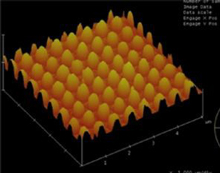
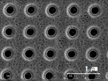
Figure 2: (a - above) AFM image of formed TiO2 nanostructure after lift-off with under-cut structure, SEM image of polymer nano-patterns after RIE process: (b - right) top-view and (c - below) cross-sectional view.
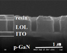
The imprinting process involves curing in UV radiation for 10 minutes at 25 atmospheres pressure. The imprint was then etched through to the ITO layer (Figure 2) with an oxygen plasma reactive-ion etch (RIE). DC magnetron sputtering was then used to deposit 100nm titanium dioxide onto the pattern that was formed, followed by a lift-off process. Dimethylformamide (DMF) solution was then used to remove the LOL under-layer. This undercutting of the under-layer was designed to prevent ‘rabbit-ear’ defects in the TiO2 nano-structures.
The structures were designed to create strong coupling to 450nm wavelength radiation and to reduce internal reflections, as determined by finite-difference time-domain (FDTD) simulations. However, the exact parameters that were used for the TiO2 was not optimized in the simulation process. In addition to the TiO2 on the ITO layer, the LEDs were grown on patterned sapphire substrates to reduce total internal reflections from the bottom surface of the LED.
LEDs were formed from the structure using lithography and etch, and gold-nickel-chromium metal electrodes were deposited. Electroluminescence studies showed that LEDs with TiO2 showed increased light emission up to 12% over devices without the structures. Current–voltage measurements confirmed that the TiO2 structure creation did not degrade the electrical performance of the devices. In particular, there was no detectable plasma-induced damage.
![]() Search: Blue LEDs GaN Sapphire substrates
Search: Blue LEDs GaN Sapphire substrates
Visit: http://jjap.jsap.jp
For more: Latest issue of Semiconductor Today
The author Mike Cooke is a freelance technology journalist who has worked in the semiconductor and advanced technology sectors since 1997.
![]() ©2010 Juno Publishing and Media Solutions Ltd. All rights reserved. Semiconductor Today and the editorial material contained within it and related media is the copyright of Juno Publishing and Media Solutions Ltd. Reproduction in whole or part without permission from Juno Publishing and Media Solutions Ltd is forbidden. In most cases, permission will be granted, if the author, magazine and publisher are acknowledged.
©2010 Juno Publishing and Media Solutions Ltd. All rights reserved. Semiconductor Today and the editorial material contained within it and related media is the copyright of Juno Publishing and Media Solutions Ltd. Reproduction in whole or part without permission from Juno Publishing and Media Solutions Ltd is forbidden. In most cases, permission will be granted, if the author, magazine and publisher are acknowledged.
Disclaimer: Material published within Semiconductor Today and related media does not necessarily reflect the views of the publisher or staff. Juno Publishing and Media Solutions Ltd and its staff accept no responsibility for opinions expressed, editorial errors and damage/injury to property or persons as a result of material published.
Semiconductor Today, Juno Publishing and Media Solutions Ltd, Suite no. 133, 20 Winchcombe Street, Cheltenham, GL52 2LY, UK
Web site by No Name No Slogan ![]()