| Home | About Us | Contribute | Bookstore | Advertising | Subscribe for Free NOW! |
| News Archive | Features | Events | Recruitment | Directory |
News
9 November 2010
Singapore researchers create amber light for nitride LEDs
Multi-quantum wells (MQWs) built of indium gallium nitride (InGaN) semiconductors are widely used to produce short-wavelength visible light from green through blue to ultraviolet. Researchers would like to fill out the red end of the visible spectrum. In principle, this could be achieved with higher indium content in the InGaN material. However, with higher indium content there is a tendency to clump into higher In and lower In regions, rather than having a homogeneous In distribution.
Researchers from Singapore’s Institute of Materials Research and Engineering (part of the Agency for Science, Technology and Research, A*STAR), and the Singapore–MIT Alliance at National University of Singapore, have been using this clumping effect to create quantum dots (QDs) with suitable longer-wavelength yellow emission properties [C. B. So et al, J. Appl. Phys., vol108, p093501, 2010]. The researchers also developed an aluminum nitride (AlN) capping layer technique to protect the dots from the high-temperature thermal processing needed to create the p-contact of light-emitting diode (LED) devices.
The researchers grew three types of three-period MQW sample on c-plane sapphire using metal-organic chemical vapor deposition (MOCVD). The barrier material consisted of GaN. The wells consisted of two InGaN layers – a 1nm ‘wetting layer’ and a 2nm layer with higher trimethyl-indium (TMIn) flow rate (and hence In content). The purpose of the wetting layer is to reduce the strain for subsequent quantum dot growth. The trimethyl-gallium (TMGa) flow rate was the same in both cases. The growth temperature was 725°C.
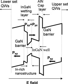 The well growth was interrupted between the layers in two of the sample types (samples B and C) to allow indium-rich quantum dots to form where TMIn flowed under ammonia-rich conditions (the nitrogen source) for 30 seconds (Figure 1). In the case of sample C, a ~1.2nm AlN layer was inserted between the wells and the GaN barrier.
Figure 1: Schematic representation of energy band profile of strained AlN/InGaN QDs/InGaN/GaN quantum well.
The aim of using the AlN layer was to reduce degradation of the QDs under further growth, through In out-diffusion for example. Also the high-temperature anneals for p-contact activation was a concern. Atomic force microscopy (AFM) morphology studies were used to understand the various growth processes and to develop improved samples.
Once the MQWs had been grown, a 10nm GaN capping layer was applied. The B and C material was used to create LEDs (samples X and Y) by adding p-AlGaN (25% Al) and p-GaN as the electron-blocking layer and p-contact, respectively. The magnesium doping was activated with a 20 minute anneal at 825°C in-situ in the growth chamber. Transmission electron microscopy (TEM) was used to understand the impact of this process on the samples. It was found that the anneal tends to shrink the QDs, but there was less of an impact in samples with AlN between the wells and the barriers.
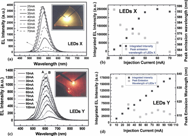
Figure 2: Current-dependent EL spectra (left) and plots (right) of the light-output power and peak emission wavelength of LEDs as a function of injection current, for LEDs X (top) and Y (bottom).
Photoluminescence studies on the QD samples without p-contact layers were carried out and it was found that a simulation anneal at 820°C blue-shifted the emission from B (without AlN caps) but red-shifted that from C (with AlN). The effect of annealing is out-diffusion of the high indium content of the dots. Without the AlN cap, the indium can diffuse also out of the well into the surrounding barrier region. However, with the cap, the indium is confined to the well region, creating longer-wavelength-emitting material there (red-shift). In the case of sample B without cap, the effect of wider indium diffusion creates a lower indium content in the well layers and also allows strain relaxation, reducing piezoelectric polarization fields. Both these factors would tend to produce a blue-shift. (Piezoelectric fields tend to create a red-shift in InGaN MQWs grown in the c-direction.)
Electroluminescence studies on the LED structures showed the devices to be yellow emitting, with broad emission bands covering wavelengths 500–680nm for sample X (without AlN caps) and 550–750nm for sample Y (with AlN). The dominant peaks of the samples blue-shifted with increasing current (30mA to 70mA): from 582nm to 562nm for sample X; and from 668nm to 658nm for sample Y. The smaller shift in sample Y is taken by the researchers as suggesting that the effect of piezoelectric fields is smaller in LED Y. Thus, it is believed that the AlN cap also reduced the strain between the InGaN well and GaN barrier for the second and third periods of the structure. This reduces the amount of polarization charge at interfaces and hence the polarization electric fields in the structure.
See related items:
Lumileds improves hot/cold factor and light output with LUXEON Rebel PC Amber LED
![]() Search: MQWs InGaN QDs Amber LEDs MOCVD TMIn TMGa
Search: MQWs InGaN QDs Amber LEDs MOCVD TMIn TMGa
Visit: http://link.aip.org
For more: Latest issue of Semiconductor Today
![]() ©2010 Juno Publishing and Media Solutions Ltd. All rights reserved. Semiconductor Today and the editorial material contained within it and related media is the copyright of Juno Publishing and Media Solutions Ltd. Reproduction in whole or part without permission from Juno Publishing and Media Solutions Ltd is forbidden. In most cases, permission will be granted, if the author, magazine and publisher are acknowledged.
©2010 Juno Publishing and Media Solutions Ltd. All rights reserved. Semiconductor Today and the editorial material contained within it and related media is the copyright of Juno Publishing and Media Solutions Ltd. Reproduction in whole or part without permission from Juno Publishing and Media Solutions Ltd is forbidden. In most cases, permission will be granted, if the author, magazine and publisher are acknowledged.
Disclaimer: Material published within Semiconductor Today and related media does not necessarily reflect the views of the publisher or staff. Juno Publishing and Media Solutions Ltd and its staff accept no responsibility for opinions expressed, editorial errors and damage/injury to property or persons as a result of material published.
Semiconductor Today, Juno Publishing and Media Solutions Ltd, Suite no. 133, 20 Winchcombe Street, Cheltenham, GL52 2LY, UK
Web site by No Name No Slogan ![]()