| Home | About Us | Contribute | Bookstore | Advertising | Subscribe for Free NOW! |
| News Archive | Features | Events | Recruitment | Directory |
News
4 May 2010
Yet another angle on nitride laser diodes
University of California Santa Barbara (UCSB) and Japan’s Mitsubishi Chemical have used semi-polar free-standing gallium nitride (GaN) substrates oriented with (30-31) surface planes (Figure 1) to create laser diodes (LDs) emitting at wavelengths of around 444nm [Po Shan Hsu et al, Appl. Phys. Express, vol.3, p052702, 2010].
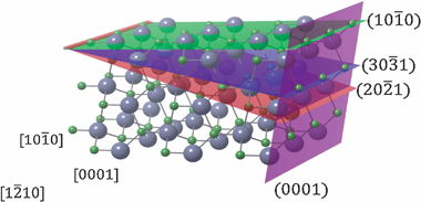
Figure 1: Wurtzite GaN crystal structure, showing (10-10), (30-31), (20-21), and (0001) planes.
Although these devices lased in the indium gallium nitride (InGaN) comfort-zone of wavelengths, the researchers are hopeful that estimated higher critical thicknesses for device layers and lower polarization effects will make (30-31) devices ‘viable candidates’ for longer-wavelength applications. Indeed, the researchers report that studies in the green spectral region are underway and that ‘further details will be published in subsequent papers’.
Many research groups are investigating different surface orientations for GaN-based light-emitting devices in the hope of finding those optimal for light emission, particularly in the harder-to-access wavelengths (e.g. green, deep ultraviolet). One particularly attractive application for green lasers would be miniature mobile projectors. Such devices would need to be highly efficient, compact, reliable, and responsive to modulation.
The easiest and most mature growth direction in GaN-based devices is the c-plane (0001). However, devices grown using this material exhibit large spontaneous and piezoelectric (strain-dependent) polarization electric fields that arise from the ionic nature of the bonds in nitride semiconductors. The polarization fields tend to separate the negative (electron) and positive (holes) carriers that need to recombine to produce light — this quantum-confined Stark effect (QCSE) decreases quantum-well (QW) radiative recombination rates, and blue-shifts the emission wavelength at higher current injection.
However, non-standard orientation substrates often have higher dislocation densities that limit performance. For example, non-polar m-plane (10-10) substrates have been limited so far to wavelengths less than 500nm due to stacking faults in the indium gallium nitride (InGaN) active regions.
The UCSB and Mitsubishi researchers have previously investigated the use of (20-21) semi-polar substrates, but found that they needed to use some quaternary aluminum indium gallium nitride (AlInGaN) compound semiconductor cladding layers that would be difficult to implement in mass production (see related item below).
The difficulties with (20-21)-grown layers was found to be misfit dislocations (MDs) that form to relieve stress in the nitride materials. The MDs are enabled by the pre-existing threading dislocations (TDs) that always exist at some level in nitride semiconductors. The internal forces that cause the TDs to glide and form MDs are largest for semi-polar planes inclined at about 45° to the basal c-plane.
The (30-31) plane has a greater inclination (Figure 1) compared with (20-21) and hence should have a lesser tendency to form MDs. This means that thicker layers can be grown before risking the formation of such dislocations. For example, Matthews–Blakeslee calculations of equilibrium critical thickness for In0.06Ga0.94N epitaxially grown on (11-22), (20-21), and (30-31) GaN semi-polar planes give 17nm, 46nm and 74nm, respectively, assuming isotropic elasticity. Thicker layers could enable greater flexibility for designing the waveguides of laser diodes.
The researchers grew an AlGaN-cladding-free laser diode on (30-31) GaN using atmospheric-pressure metal-organic chemical vapor deposition. A typical structure was used: thick GaN lower cladding, silicon-doped InGaN waveguide, three periods of undoped InGaN/GaN QW/barrier, magnesium-doped (Mg-doped) AlGaN electron-blocking layer (EBL), Mg-doped InGaN upper waveguide, Mg-doped GaN upper cladding, and Mg-doped GaN p++ contact. Photolithography and etching were used to create ridge waveguide LDs with palladium-gold p-electrodes and back-side aluminum-gold n-electrodes.
The devices emitted light at the short-wavelength end of the blue range (440–490nm) with a laser threshold current of ~1022mA (~5.6kA/cm2). The rather high threshold voltage of 9.9V was blamed on ‘unoptimized p-contacts and doping profiles’. The devices were tested with pulsed currents (1μsec, 0.1% duty cycle).
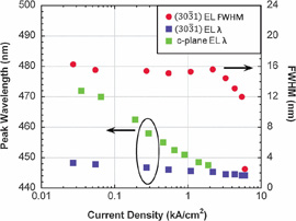 Figure 2: Peak wavelength and FHWM dependence on current density. Peak wavelength data for a 450nm c-plane LD is included for comparison.
Below the lasing threshold the electroluminescence wavelength was 448nm at an injection current of 0.03kA/cm2 (Figure 2). Just above threshold, the wavelength was blue-shifted some 4nm to 444nm at 6.0kA/cm2. A c-plane device that lases at the same wavelength would typically have a below-threshold value as low as ~470nm. The 4nm shift is comparable to that observed in non-polar m-plane devices.
The characteristic temperature of the threshold current (T0) was estimated to be ~135K, using measurements in the range 20–50°C when the output power was about 35mW. ‘This value compares well to those reported for c-plane devices emitting at the same wavelength range,’ the researchers comment. The variation of the peak wavelength with temperature was ~0.06nm/K, also corresponding well with values given for m-plane, c-plane, and (20-21)-plane devices.
Funding for the research came from US National Science Foundation (NSF) National Nanotechnology Infrastructure Network and the NSF’s Materials Research Science and Engineering Center, and from UCSB’s Solid State Light and Energy Center. Shuji Nakamura, one of the pioneers of nitride semiconductor devices, is one of the authors of the paper.
See related items:
AlGaN-cladding-free semipolar laser nears green
![]() Search: Laser diodes Semi-polar free-standing GaN substrates InGaN
Search: Laser diodes Semi-polar free-standing GaN substrates InGaN
Visit: http://apex.ipap.jp/link?APEX/3/052702
The author Mike Cooke is a freelance technology journalist who has worked in the semiconductor and advanced technology sectors since 1997.
![]() ©2010 Juno Publishing and Media Solutions Ltd. All rights reserved. Semiconductor Today and the editorial material contained within it and related media is the copyright of Juno Publishing and Media Solutions Ltd. Reproduction in whole or part without permission from Juno Publishing and Media Solutions Ltd is forbidden. In most cases, permission will be granted, if the author, magazine and publisher are acknowledged.
©2010 Juno Publishing and Media Solutions Ltd. All rights reserved. Semiconductor Today and the editorial material contained within it and related media is the copyright of Juno Publishing and Media Solutions Ltd. Reproduction in whole or part without permission from Juno Publishing and Media Solutions Ltd is forbidden. In most cases, permission will be granted, if the author, magazine and publisher are acknowledged.
Disclaimer: Material published within Semiconductor Today and related media does not necessarily reflect the views of the publisher or staff. Juno Publishing and Media Solutions Ltd and its staff accept no responsibility for opinions expressed, editorial errors and damage/injury to property or persons as a result of material published.
Semiconductor Today, Juno Publishing and Media Solutions Ltd, Suite no. 133, 20 Winchcombe Street, Cheltenham, GL52 2LY, UK
Web site by No Name No Slogan ![]()