| Home | About Us | Contribute | Bookstore | Advertising | Subscribe for Free NOW! |
| News Archive | Features | Events | Recruitment | Directory |
News
21 May 2010
Nano-patterned silicon substrate gives higher output power nitride LEDs
Hong Kong University of Science and Technology and Taiwan National Chiao Tung University researchers report lower leakage current and higher light output power for violet (380-450nm) indium gallium nitride (InGaN) light emitting diodes grown on nano-patterned silicon substrates, compared with those grown on Si substrates with micro-scale patterning [Dongmei Deng et al, Appl. Phys. Lett., vol96, p201106, 2010]
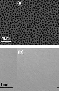 The nano-patterning was achieved with an anodized aluminum oxide (AAO) etch mask giving a pore diameter of 150nm and a separation of 120nm, on average (Figure 1). The use of such substrates encourages nano-hetero-epitaxial lateral overgrowth giving higher crystal quality in the subsequent nitride semiconductor layers, improving performance.
Figure 1: (a) Top-view SEM of nano-patterned Si. (b) Optical micrograph of LED surface grown on nano-patterned Si.
The attraction of silicon substrates is the lower manufacturing costs from both the raw material and economies of scale from the larger wafer sizes available. A further attraction over the sapphire substrates more often used for nitride semiconductor growth is the higher thermal conductivity of silicon that allows better thermal control of devices.
The lattice mismatch of GaN with Si is ~17%, compared with the ~14% for sapphire and ~3% for silicon carbide. Large mismatches lead to a high defect density of 109-1011/cm2 for GaN/Si. Commercial GaN substrates typically specify defect densities less than 109/cm2.
The researchers had previously developed micro-scale patterning using a silicon nitride (SiN) mask. Some improvement in GaN layers was achieved, but the SiN deposition process can be difficult to control in terms of thickness and surface uniformity/flatness. The researchers were attracted to the self-ordering AAO process as being a low-cost, high throughput way of creating nano-patterning, compared with the use of lithography.
The AAO mask was formed on 2-inch Si (111) wafers at 6°C in 0.3M phosphoric acid with 120V applied for 30mins. The pattern was transferred to the underlying Si substrate using inductively coupled plasma (ICP) etching. The AAO mask was removed using a wet etch.
LED structures were grown using metal-organic chemical vapor deposition (MOCVD). Devices on micro-scale patterned templates (340x340μm grid-pattern separated by 20μm trenches, SiN mask) were also made for comparison.
The buffer consisted of aluminum gallium nitride (AlGaN), starting with a ~40nm AlN nucleation layer, 200nm AlGaN and 800nm undoped GaN, and finally a 250nm AlGaN/AlN interlayer. Then a 1μm thick n-type silicon-doped GaN contact layer was deposited. A five-period InGaN/GaN quantum well was grown as the active layer. The final p-type contact layer consisted of Mg-doped GaN.
Optical microscopic inspection of the resulting wafers showed the material to be crack-free, and the surface was described as being ‘mirror-like’. Closer analysis with transmission electron microscopy (TEM) showed threading dislocations, but the density was less in the nano-patterned sample, compared with the micro-patterned one.
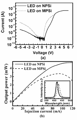 Both samples were used to form 300x300μm LEDs. The forward voltage of the both devices was ~4.7V at 20mA. Much lower leakage currents were observed at reverse bias for the nano-patterned device (Figure 2). The output power at 20mA was 1.28mW for the nano-patterning, a 21% improvement over the micro-patterned material. Also the nano-patterned LED saturation current was 110mA, compared with 90mA for the micro-patterned device.
Figure 2: (a) Current-voltage (I-V) characteristics of nano- (NPSi) and micro-patterned silicon (MPSi) LEDs. (b) Light output power-current (L-I) curves with (inset) electroluminescence (EL) spectra at 20mA injection current.
The emission wavelength of the nano-pattern LED was blue-shifted compared with the micro-LED. This was expected from Raman spectral analyses of the material carried out before the LED structures were made. The researchers believe that the blue-shift indicates stress relief in the nano-patterned samples, making higher quality, low defect material layers easier to grow.
![]() Search: InGaN LEDs Silicon substrates
Search: InGaN LEDs Silicon substrates
Visit: http://link.aip.org/link
The author Mike Cooke is a freelance technology journalist who has worked in the semiconductor and advanced technology sectors since 1997.
![]() ©2010 Juno Publishing and Media Solutions Ltd. All rights reserved. Semiconductor Today and the editorial material contained within it and related media is the copyright of Juno Publishing and Media Solutions Ltd. Reproduction in whole or part without permission from Juno Publishing and Media Solutions Ltd is forbidden. In most cases, permission will be granted, if the author, magazine and publisher are acknowledged.
©2010 Juno Publishing and Media Solutions Ltd. All rights reserved. Semiconductor Today and the editorial material contained within it and related media is the copyright of Juno Publishing and Media Solutions Ltd. Reproduction in whole or part without permission from Juno Publishing and Media Solutions Ltd is forbidden. In most cases, permission will be granted, if the author, magazine and publisher are acknowledged.
Disclaimer: Material published within Semiconductor Today and related media does not necessarily reflect the views of the publisher or staff. Juno Publishing and Media Solutions Ltd and its staff accept no responsibility for opinions expressed, editorial errors and damage/injury to property or persons as a result of material published.
Semiconductor Today, Juno Publishing and Media Solutions Ltd, Suite no. 133, 20 Winchcombe Street, Cheltenham, GL52 2LY, UK
Web site by No Name No Slogan ![]()