| Home | About Us | Contribute | Bookstore | Advertising | Subscribe for Free NOW! |
| News Archive | Features | Events | Recruitment | Directory |
News
5 March 2010
Pushing AlInN and AlGaN HEMTs further on SiC and silicon
The Terahertz Electronics Group of the Swiss Federal Institute of Technology Zurich (ETH-Zürich) has made progress, collaborating with other groups, in producing nitride semiconductor high-electron-mobility transistors (HEMTs) with performance characteristics beyond 100GHz (0.1THz). The group believes that such components could lead to high-power and high-speed performance, even in higher-temperature environments.
With Institute of Quantum Electronics and Photonics, Ecole Polytechnique Fédérale de Lausanne (EPFL), aluminum indium nitride on gallium nitride (AlInN/GaN) devices with a cut-off frequency (fT) of 144GHz with 100nm gate length have been developed on semi-insulating silicon carbide (SiC) substrates [Haifeng Sun et al, IEEE Electron Device Letters, published online 22 February 2010]. Using high-resistivity (111) silicon (HR-Si, 20kΩ-cm) substrates and a similar device structure, the same research achieved an fT of 113GHz. Looking to lower costs, AlGaN/GaN devices on high-resistivity (111) Si (10kΩ-cm) substrates have also been developed with Nitronex, exhibiting an fT of 107GHz [Stefano Tirelli et al, IEEE Electron Device Letters, published online 25 February 2010].
The ETH-Zürich/EPFL work used the newer, less mature AlInN/GaN heterojunction since this format is predicted to yield higher transconductance and current density values compared with AlGaN/GaN heterojunctions. The AlInN layers can be more nearly lattice matched with GaN, compared with AlGaN/GaN. While initial work has confirmed the expectations of better transconductance and current density, the frequency bandwidth performance has previously lagged behind the AlGaN/GaN reports. Now, the ETH-Zürich/EPFL team has not only beaten the previous fT high of 102GHz for AlInN/GaN devices with 100nm gate length, it has also managed to match the best published values for AlGaN/GaN HEMTs, even those with an insulated gate.
The metal-organic chemical vapor deposition (MOCVD) growth of the epitaxial layers on the respective substrates was carried out at EPFL: beginning with a 30nm aluminum nitride (AlN) nucleation layer, 1μm GaN insulating buffer and channel, 1nm AlN spacer, and finishing with a 10nm Al0.83In0.17N barrier. The SiC epitaxial wafers had channel electron sheet densities of 2.4x10¹³/cm2 and mobility of 1300cm 2/V-s, measured using the Hall effect. The corresponding values for the HR-Si structures were
1.95x10¹³/cm2 and mobility of 1060cm 2/V-s, respectively.
The resulting sheet resistances were 200Ω/sq (SiC) and 300Ω/sq (HR-Si), improving the values from the group’s previous work by 2–3x. This has been enabled by improving the material quality, particularly at the AlInN/GaN interface. This was achieved by optimizing the buffer layer thickness and the growth temperatures.
Devices were formed using chlorine/methane/helium/argon plasma to etch 200nm isolation mesas and evaporating titanium/aluminum/gold (Ti/Al/Au) ohmic source/drain contacts (resistances of 0.48Ω-mm on SiC, 0.49Ω-mm on HR-Si). The 100nm T-gates of nickel/gold (Ni/Au) were formed using electron-beam lithography and lift-off techniques. A 100nm plasma-enhanced CVD silicon nitride passivation was used, along with Ti/Au overlay metallization on the ohmic and gate metal contacts.
The maximum drain current for a 2x(0.1x75μm) device on SiC was 1.84A/mm with zero gate–source potential difference (VGS = 0V), while the maximum extrinsic transconductance was 480mS/mm (VDS = 4V).
Complete channel pinch-off was not achieved due to residual gate leakage. Buffer leakage is excluded as the reason for the soft pinch-off by the experimenters due to the high isolation between the mesas (greater than 1010Ω/sq). Gate leakage is commonly observed in AlInN/GaN HEMTs with thin AlInN barrier layers. The reasons for the gate leakage are being investigated; the researchers would also like to find a suitable gate insulator, as opposed to using a Schottky contact with the AlInN barrier. The maximum current and extrinsic transconductance for similar HR-Si devices were 1.43A/mm and 335mS/mm with the same bias conditions.
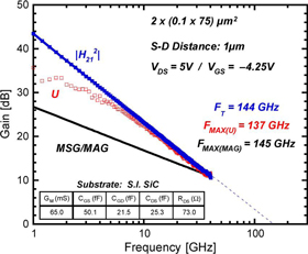 Figure 1: Microwave performance for 2 x (0.1x75μm) AlInN/GaN HEMTs on SiC (a - right) and HR-Si (b - below) produced by ETH-Zürich/EPFL. Extrapolations at –20dB/dec.
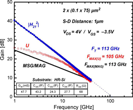 Radio-frequency measurements were carried out from DC to 40GHz (Figure 1). Measurements with VDS of 5V and VGS of -4.25V give, in addition to the fT value of 144GHz, a maximum oscillation frequency of 137GHz (fMAX(U)) based on extrapolation of Mason’s unilateral gain (145GHz for maximum available gain, fMAX(MAG)). The HR-Si values were 113GHz (fT), 105GHz (f MAX(U)) and 113GHz (fMAX(MAG)) at VDS of 4V and VGS of -3.5V.
The ETH-Zürich/Nitronex work involved AlGaN/GaN/Si epitaxial wafers grown at Nitronex’ facility. The base 100mm-diameter substrate was a high-resistivity (111) Si (10kΩ-cm) substrate. The insulating buffer/channel GaN was 1.7μm thick. The barrier layer was 17.5nm Al0.26Ga0.74N. A 2nm GaN cap layer was also deposited. The resulting mobility was about 1500cm2/V-s. HEMT devices were constructed with mesa isolation, Ti/Al/Au ohmic contacts, and Ni/Au T-gate lengths of 75nm and 100nm (200nm and 400nm T-heads, respectively). The source–drain distances were 2μm and 1μm for the 75nm and 100nm gate-length devices, respectively. SiN passivation of 100nm thickness was applied with PECVD and Ti/Au overlay metal with evaporation/lift-off.
The maximum drain current and extrinsic transconductance (VDS = 3V) were 705mA/mm and 285mS/mm, respectively, for the 75nm gate length. The respective figures for the 100nm device were 750mA/mm and 310mS/mm. The lower 75nm values were attributed to the large source–drain distance. Complete channel pinch-off was achieved at VGS values of -3.5V and -3.3V for the 75nm and 100nm devices, respectively. The breakdown characteristics BVGD, with a current threshold of 1mA/mm, were 58V and 30V for 75nm and 100nm devices, respectively. The shorter source–drain distance in the latter case increases the electric field in the device.
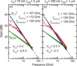 Figure 2: Microwave performance for 75nm (a) and 100nm (b) for AlGaN/GaN HEMTs produced by ETH-Zürich/Nitronex. Extrapolations at –20dB/dec.
RF measurements were carried out between 0.2GHz and 40.2GHz. These revealed fMAX(MSG)/fT values of 128GHz/107GHz and 128GHz/101GHz for the 75nm and 100nm HEMTs, respectively (Figure 2). According to the authors, these results supersede previous records for such devices built on HR-Si substrates. ‘The peak fT = 107GHz with the LG = 75 nm gate HEMT is, to the best of our knowledge, the highest cutoff frequency value ever reported for fully passivated (Al,Ga)N/GaN or (Al,In)N/GaN HEMTs on HR-Si.’ [The ETH-Zürich/Nitronex paper was submitted about two weeks before the ETH-Zürich/EPFL work discussed above.] The results also compare favorably with similar devices built on more traditional SiC substrates.
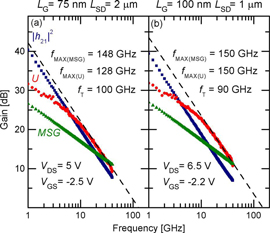 Figure 3: Microwave performance with increased drain bias for 75nm (a) and 100nm (b) for AlGaN/GaN HEMTs produced by ETH-Zürich/Nitronex. Extrapolations at –20dB/dec.
The maximum oscillation frequency can be increased from the 128GHz value with a higher drain voltage (Figure 3): the 75nm device can reach 148GHz (fMAX(MSG), fMAX(U) = 128GHz); and the 100nm HEMT gives 150GHz (and also fMAX(U) = 150GHz). These are ‘unprecedented’ values for HR-Si devices with fT more than 90GHz (although not for SiC-based components with no or ultrathin passivation).
See related items:
Seeking ultra-low ohmic path to high-frequency nitride transistors
Gate control of terahertz transistor emission frequency
Reducing GaN HEMT degradation with InAlN barrier
![]() Search: AlInN HEMTs AlGaN HEMTs SiC substrates
Search: AlInN HEMTs AlGaN HEMTs SiC substrates
Visit: www.mwe.ee.ethz.ch/en
Visit: http://dx.doi.org/10.1109/LED.2009.2039845
Visit: http://dx.doi.org/10.1109/LED.2009.2039847
The author Mike Cooke is a freelance technology journalist who has worked in the semiconductor and advanced technology sectors since 1997.
![]()
![]() ©2010 Juno Publishing and Media Solutions Ltd. All rights reserved. Semiconductor Today and the editorial material contained within it and related media is the copyright of Juno Publishing and Media Solutions Ltd. Reproduction in whole or part without permission from Juno Publishing and Media Solutions Ltd is forbidden. In most cases, permission will be granted, if the author, magazine and publisher are acknowledged.
©2010 Juno Publishing and Media Solutions Ltd. All rights reserved. Semiconductor Today and the editorial material contained within it and related media is the copyright of Juno Publishing and Media Solutions Ltd. Reproduction in whole or part without permission from Juno Publishing and Media Solutions Ltd is forbidden. In most cases, permission will be granted, if the author, magazine and publisher are acknowledged.
Disclaimer: Material published within Semiconductor Today and related media does not necessarily reflect the views of the publisher or staff. Juno Publishing and Media Solutions Ltd and its staff accept no responsibility for opinions expressed, editorial errors and damage/injury to property or persons as a result of material published.
Semiconductor Today, Juno Publishing and Media Solutions Ltd, Suite no. 133, 20 Winchcombe Street, Cheltenham, GL52 2LY, UK
Web site by No Name No Slogan ![]()