| Home | About Us | Contribute | Bookstore | Advertising | Subscribe for Free NOW! |
| News Archive | Features | Events | Recruitment | Directory |
News
7 June 2010
Sapphire to exceed 50% of compound semiconductor substrate processed surface area from 2011
Driven by the booming business in white LEDs for LCD backlights and general illumination, from 2011 sapphire will become the leading compound semiconductor substrate material in terms of volume, exceeding 50% of total compound semiconductor processed surface area, according to the new report ‘Compound Semiconductor Substrates 2010’ from market research firm Yole Développement.
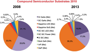
Graphic credit: Yole Développement, May 2010.
Up to now, thanks to wireless technology and demand for red/orange/yellow LEDs, GaAs has been the leading compound semiconductor material by processed surface area, accounting for 56.9% of the total (31.1% semi-insulating and 25.8% semiconducting), compared to 33% for sapphire. However, in 2013, this will be 55.3% for sapphire and 36.9% for GaAs (19.9% semi-insulating and 17% semiconducting), forecasts Yole.
Silicon still dominates the semiconductor industry as the standard material, with gallium arsenide (GaAs), indium phosphide (InP), gallium phosphide (GaP), gallium nitride (GaN), silicon carbide (SiC) and sapphire substrates currently accounting for just 1.1% of the 7504 million square inches processed annually in semiconductor foundries. However, specific applications such as optoelectronics, RF wireless and power electronics require device performance (i.e. frequency, power, thermal conductivity, robustness, junction temperature, voltage breakdown etc) that is not reachable by using the material properties of silicon, so compound semiconductor materials have been protected from competition from silicon.
Hence, even though compound materials have much higher market prices than silicon, their technical specifications have been — and will remain — the main driver for the adoption of compound semiconductor substrates and related technologies.
Also, the small portion of total semiconductor processed area for compound semiconductors is compensated by their higher merchant prices, leading to a raw substrate market of $880m in 2009. This should reach the billion dollar threshold in 2010.
Yole notes that all the compound semiconductor materials covered in the report are now available in sizes up to and including 4-inches in diameter (except for bulk GaN, which has just been made available at 3-inches in diameter in Japan). Such diameter expansion helps to lower manufacturing costs for compound semiconductor-based devices and facilitates the mass marketing of affordable products, the firm adds.
See related items:
Sapphire faces shortage in second-half 2010, to be resolved in early 2011
Sapphire substrate market to grow at 21% to $400m by 2012
Compound semiconductor substrate market to top $1bn by 2009-2010
![]() Search: Substrate market
Search: Substrate market
Visit: www.yole.fr
![]() ©2010 Juno Publishing and Media Solutions Ltd. All rights reserved. Semiconductor Today and the editorial material contained within it and related media is the copyright of Juno Publishing and Media Solutions Ltd. Reproduction in whole or part without permission from Juno Publishing and Media Solutions Ltd is forbidden. In most cases, permission will be granted, if the author, magazine and publisher are acknowledged.
©2010 Juno Publishing and Media Solutions Ltd. All rights reserved. Semiconductor Today and the editorial material contained within it and related media is the copyright of Juno Publishing and Media Solutions Ltd. Reproduction in whole or part without permission from Juno Publishing and Media Solutions Ltd is forbidden. In most cases, permission will be granted, if the author, magazine and publisher are acknowledged.
Disclaimer: Material published within Semiconductor Today and related media does not necessarily reflect the views of the publisher or staff. Juno Publishing and Media Solutions Ltd and its staff accept no responsibility for opinions expressed, editorial errors and damage/injury to property or persons as a result of material published.
Semiconductor Today, Juno Publishing and Media Solutions Ltd, Suite no. 133, 20 Winchcombe Street, Cheltenham, GL52 2LY, UK
Web site by No Name No Slogan ![]()