| Home | About Us | Contribute | Bookstore | Advertising | Subscribe for Free NOW! |
| News Archive | Features | Events | Recruitment | Directory |
News
2 June 2010
Large chip improvements to deep-ultraviolet output power
Sensor Electronic Technology (SET) has reported details of their achievement of continuous-wave (CW) 6mW and 30mW light output power from single-chip light-emitting diodes (LEDs) operating at wavelengths of 247nm and 273nm, respectively [Max Shatalov et al, Appl. Phys. Express, vol3, p062101, 2010]. In addition to the SET researchers, two scientists from the US Army Research Lab also contributed to the work.
Potential applications for such devices include defense/security, bio-analysis, medical, chemical sensors, and curing of materials. The deep-ultraviolet (DUV) wavelengths (<300nm) are particularly being developed for non-thermal disinfectant/sterilization of water and other materials, and decontamination of surfaces. Short-wavelength light (~260nm) disrupts DNA structures, killing micro-organisms.
Recent work at SET to increase light output power (L) has focused on creating larger-area chips. The company uses metal-organic chemical vapor deposition (MOCVD) and SET’s own migration-enhanced MOCVD (MEMOCVD) processes to create the diode layers on sapphire substrates. The final chips were 0.5mm2 or 1mm2 in area.
The metallization was performed on 100μm mesas (Figure 1) formed through reactive ion etch (RIE) processing. The aim was to create uniform current spreading. The large chip sizes help in heat dissipation from the junction. The n-contact consisted of chromium/titanium/gold (Cr/Ti/Au) layers that were annealed in nitrogen above 850°C. Linear transfer length model measurements give a contact resistance of 5x10⁻⁵Ω-cm2 on the Al0.6Ga0.4N layers used in the n-contacts of the 273nm devices. This increased to 10-4Ω-cm2 for the Al0.8Ga0.2N layers of the 247nm LED. The p-contact consisted of nickel/gold (Ni/Au) annealed in air at 500°C.
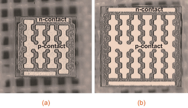
Figure 1: Microscope image of DUV LED chips with junction area of (a) 0.5mm2 and (b) 1mm2.
The devices were separated using laser scribing and packaged into TO-3 cans with a customized copper heatsink. Use of the larger-junction chips resulted in a significant reduction of forward voltages (6.5V at 700mA, with maximum CW light output power of nearly 30mW with no special thermal management measures, short pulsing of 1μsec gave 65mW at 1.4A), giving a differential resistance (Rd) of less than 1Ω. Measurements of various chip sizes at a current of 20mA give a differential resistance that is inversely proportional to the junction area between 0.035mm2 and 1mm2. The researchers comment that this indicated that the dominant contributions to this resistance come from the p–n junction and the p-contact. The larger devices were limited in further reduction of differential resistance to 10Ω at 20mA due to problems with current spreading in the n-AlGaN layer.
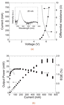 The emission spectrum of the 273nm device at 20mA (Figure 2) has a full-width half-maximum (FWHM) of 10nm, with the secondary peak at ~420nm suppressed by more than three orders of magnitude. This suggests good confinement of injected carriers into the multi-quantum-well active region, rather than allowing overshoots into regions where longer-wavelength recombination takes place.
Figure 2: (a) CW I–V and Rd–I characteristics of 1mm2 DUV LED with 273nm emission. Inset: LED emission spectrum at 20mA CW. (b) L–I and EQE–I characteristics of 0.035mm2 (open symbols) and 1mm2 (closed symbols) DUV LEDs.
The external quantum efficiency (EQE) performance at higher currents is also much improved for the 273nm device (Figure 2). The smaller devices peak at about 1.3% EQE but fall off rapidly. For the larger device the EQE also peaks at about 1.3% (wall-plug efficiency/WPE 1%) at a higher current ~100mA, but falls off much more slowly. The difference in performance is blamed on joule heating in the smaller device at high currents.
The reduced power at shorter wavelengths is largely attributed to the poorer material quality of the high-Al-content AlGaN layers needed to create higher-energy photons. The operating voltage also increases due to the higher resistance of the contacts and AlGaN layers. Due to higher concentrations of non-radiative recombination centers, the current density needed for the peak EQE in the 247nm device was higher. To enable this higher current density, the researchers used a smaller 0.5mm2 area chip.
Operation at a CW 200mA forward current (10V) resulted in 5mW light output, corresponding to an EQE of 0.5% and WPE of 0.25%. The big reduction in WPE is blamed on the joule losses associated with the higher voltage drops across the contact and barrier layers in these devices. The researchers believe that new doping approaches and contact fabrication processes need to be investigated with a view to reducing these losses in efficiency.
In terms of the spectral output, the 247nm devices were similar in performance to the 273nm LEDs, with an FWHM of 10nm and a suppression factor of 500 for the secondary peak.
The reliability of a 0.5mm2 273nm device was also evaluated in quasi-CW operation (400μsec pulses with 10% duty cycle) at 400mA. Accelerated stressing at around 100°C was achieved by packaging the device without a heat-sink. The initial output of 26mW increased to 31mW after 250 hours, and then returned to 26mW after 1500 hours. The initial increase is attributed to an annealing effect of the temperature on the p-type layers, increasing hole injection into the active layers. Using an extrapolation of the fall-off, the researchers give a time to 50% power of almost 5000 hours.
The researchers have carried out research into the degradation mechanisms for these devices [Craig G. Moe et al, Appl. Phys. Lett., vol96, p213512, 2010], finding that the electrical properties of the p-type layers change over time, reducing carrier injection and hence output power.
Partial funding for the research came from US Army Research Office contracts and Army Research Laboratory Cooperative Research Agreements.
See related items:
Deep ultraviolet power boost at shorter wavelengths
SET wins $500,000 SBIR award from NSF to advance deep UV LEDs
SET claims record performance for large-area single-chip deep UV LEDs
![]() Search: Sensor Electronic Technology LEDs Deep-ultraviolet LEDs AlGaN
Search: Sensor Electronic Technology LEDs Deep-ultraviolet LEDs AlGaN
Visit: http://apex.ipap.jp
Visit: www.s-et.com
The author Mike Cooke is a freelance technology journalist who has worked in the semiconductor and advanced technology sectors since 1997.
![]() ©2010 Juno Publishing and Media Solutions Ltd. All rights reserved. Semiconductor Today and the editorial material contained within it and related media is the copyright of Juno Publishing and Media Solutions Ltd. Reproduction in whole or part without permission from Juno Publishing and Media Solutions Ltd is forbidden. In most cases, permission will be granted, if the author, magazine and publisher are acknowledged.
©2010 Juno Publishing and Media Solutions Ltd. All rights reserved. Semiconductor Today and the editorial material contained within it and related media is the copyright of Juno Publishing and Media Solutions Ltd. Reproduction in whole or part without permission from Juno Publishing and Media Solutions Ltd is forbidden. In most cases, permission will be granted, if the author, magazine and publisher are acknowledged.
Disclaimer: Material published within Semiconductor Today and related media does not necessarily reflect the views of the publisher or staff. Juno Publishing and Media Solutions Ltd and its staff accept no responsibility for opinions expressed, editorial errors and damage/injury to property or persons as a result of material published.
Semiconductor Today, Juno Publishing and Media Solutions Ltd, Suite no. 133, 20 Winchcombe Street, Cheltenham, GL52 2LY, UK
Web site by No Name No Slogan ![]()