| Home | About Us | Contribute | Bookstore | Advertising | Subscribe for Free NOW! |
| News Archive | Features | Events | Recruitment | Directory |
News
23 June 2010
InAlN barrier strain used to shift nitride transistor thresholds
Researchers at Georgia Institute of Technology have used polarization and strain effects to shift the threshold of nitride semiconductor field-effect transistors (FETs) into enhancement mode [Suk Choi et al, Appl. Phys. Lett., vol96, p243506, 2010].
Nitride semiconductor hetero-structure FETs (HFETs, also known as high-electron-mobility transistors or HEMTs) usually operate in depletion mode, where the channel is conducting when the gate potential is 0V (normally-off). These devices have excellent high-frequency and power performance, even at high temperature, creating opportunities in military and commercial applications (e.g. mobile communication network transmission power amplification).
Some researchers have begun looking to nitrides for voltage-switching and digital opportunities. These applications are often best served by normally-off (enhancement-mode) operation to reduce power consumption in the idle state.
A number of techniques have been used to shift the threshold voltage in aluminum gallium nitride/gallium nitride (AlGaN/GaN) devices, such as low-aluminum content of the AlGaN barrier, recessed gates, fluoride plasma treatment, p-type gates, and non-polar materials.
Recently, indium aluminum nitride (InAlN) material quality has improved to the level where some researchers are exploring its use in nitride semiconductor devices. Among the new possibilities that the material opens up are HFETs on GaN with a lattice-matched InAlN barrier (with an estimated indium content of about 18%, based on a simple ‘Vegard Law’ linear interpolation). Further, InAlN barriers with in-plane compressive strain are possible, unlike in AlGaN, which is always in tension on GaN. This is the feature that Georgia Tech used to shift the threshold voltage to enhancement mode.
Strain has a particularly strong piezoelectric effect in nitride semiconductors. This is in addition to the spontaneous electric polarization fields that arise from the more ionic nature of nitride semiconductor bonds compared with more traditional semiconductors such as silicon or even gallium arsenide.
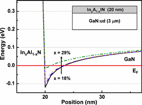 Figure 1:. Calculated electronic band diagrams of the InAlN/GaN HFET structures with various InAlN layer compositions: solid line for 18% In; dashed line for 22%; dotted line for 25%; and dashed-dotted line for 29%. As the dip below the Fermi level (EF) at the InAlN/GaN interface becomes shallower, the ability to form a 2DEG channel at zero gate potential is reduced.
The Georgia Tech researchers performed simulations (Figure 1) and created actual InAlN/GaN structures using metal-organic chemical vapor deposition (MOCVD). The HFET structures were grown on sapphire substrates and consisted of an iron-doped semi-insulating GaN layer (400nm), an unintentionally doped GaN layer (2.6μm), an unintentionally doped AlN layer (1nm) and an unintentionally doped InAlN barrier (20nm).
The purpose of the AlN layer was two-fold: to enhance carrier mobility in the two-dimensional electron gas (2DEG) channel when the transistor was ‘on’, and to protect the GaN surface during cooling from its growth temperature of 1050°C to the lower temperature needed for InAlN growth.
The In content of the InAlN layers was determined using x-ray diffraction. These measurements determine differences in the c-direction parameter, which is different than that for GaN even when the layers are lattice matched. However, the relation of this measurement to In content is rather uncertain, since a simulation that is rather sensitive to the Poisson ratio (relating in-plane and perpendicular c-direction strains) needs to be used to extract a value. The researchers therefore give a rather large error bar for the In mole fraction for unstrained InAlN/GaN of 14–22%. However, the corresponding author on the paper, Jae-Hyun Ryou, comments that the relative indium contents between the various samples should be reliable.
Three samples were measured for sheet resistance and carrier mobility (Table 1). The sample with the highest In content (25%) had a very high sheet resistance (~50kΩ/sq), which is attributed to the depletion of the 2DEG. The source of the mobility decrease is less clear, although localized state formation is a possible cause.
In content |
Sheet resistance |
Sheet carrier concentration |
Hall mobility |
|
Sample |
% |
Ω/sq |
x1012/cm2 |
cm2/V-s |
A |
~18 |
255 |
−15.7 |
1110 |
B |
~22 |
879 |
−4.89 |
683 |
C |
~25 |
> 50k |
. . . |
. . . |
Table 1: Contactless sheet resistance and Hall-effect measurement results for InAlN/GaN HFET structures with various In compositions in InAlN barrier layer.
Localized states are thought to often form in InGaN material used in producing visible light-emitting devices. These states form in regions where the In fraction varies due to segregation effects. “In fact, thermodynamic calculations suggest that InAlN is more prone to form localized states than InGaN,” comments Ryou. “However, we have not seen clear peak separation in x-ray diffraction from our samples containing InAlN with a thickness of ~20 nm — we only observed a rather broad single peak, possibly due to the thinness of the InAlN layer. This is the case even for InGaN, unless we grow a very thick layer, Ryou adds. “This segregation effect on the mobility, together with actual existence/evidence of indium segregation, requires further study.”
HFETs were created from the epitaxial material with ohmic source–drain contacts of titanium-aluminum-titanium-gold and a Schottky gate contact of nickel. The gate length was 3μm.
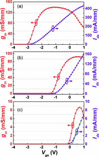 By varying the indium content of the InAlN barrier, the threshold voltage (determined by linear extrapolation of the drain current around the point of maximum transconductance, gm, Figure 2) increased from –2.5V at 18% to +0.2V at 25%. At a gate potential of 1.5V, the 25% In barrier enhancement-mode device had a relatively high on-resistance of 354Ω-mm.
Figure 2: DC transfer characteristics of 3μm gate-length InAlN/GaN HFETs with various InAlN layer compositions: (a) 18%, (b) 22%, and (c) 25%. The source–drain voltage was 5V.
The Georgia Tech researchers want to develop devices with 2DEG conducting regions under the source and drain, so that parasitic resistances are reduced, while maintaining the positive threshold under the gate for enhancement-mode characteristics. The researchers also promise to explore “further electronic band engineering and epitaxial structure development”.
See related item:
InAlN provides better electron-blocking layer in nitride LEDs
![]() Search: Georgia Institute of Technology InAlN barrier Nitride FETs
Search: Georgia Institute of Technology InAlN barrier Nitride FETs
Visit: http://link.aip.org
The author Mike Cooke is a freelance technology journalist who has worked in the semiconductor and advanced technology sectors since 1997.
![]() ©2010 Juno Publishing and Media Solutions Ltd. All rights reserved. Semiconductor Today and the editorial material contained within it and related media is the copyright of Juno Publishing and Media Solutions Ltd. Reproduction in whole or part without permission from Juno Publishing and Media Solutions Ltd is forbidden. In most cases, permission will be granted, if the author, magazine and publisher are acknowledged.
©2010 Juno Publishing and Media Solutions Ltd. All rights reserved. Semiconductor Today and the editorial material contained within it and related media is the copyright of Juno Publishing and Media Solutions Ltd. Reproduction in whole or part without permission from Juno Publishing and Media Solutions Ltd is forbidden. In most cases, permission will be granted, if the author, magazine and publisher are acknowledged.
Disclaimer: Material published within Semiconductor Today and related media does not necessarily reflect the views of the publisher or staff. Juno Publishing and Media Solutions Ltd and its staff accept no responsibility for opinions expressed, editorial errors and damage/injury to property or persons as a result of material published.
Semiconductor Today, Juno Publishing and Media Solutions Ltd, Suite no. 133, 20 Winchcombe Street, Cheltenham, GL52 2LY, UK
Web site by No Name No Slogan ![]()