| Home | About Us | Contribute | Bookstore | Advertising | Subscribe for Free NOW! |
| News Archive | Features | Events | Recruitment | Directory |
News
22 July 2010
Tuning GaN growth for Schottky barrier diodes with record figure of merit
Researchers at Japan’s Sumitomo Electric Industries Ltd (SEI) have created nitride semiconductor vertical Schottky barrier diodes (SBDs) with low specific on-resistance of 0.71mΩcm2 and high breakdown voltage of 1100V [Yu Saitoh et al, Appl. Phys. Express, vol3, p081001, 2010].
Nitride semiconductors are of increasing interest as an electronic material capable of handling high power, high frequency and high temperature. These applications use the interconnected characteristics of large energy bandgap, high breakdown field and high saturation electron velocity. Potential applications include high-frequency power amplification for mobile phone network base-station transmissions and power switching devices.
The latest Sumitomo results were achieved by creating high-quality n-type gallium nitride (GaN) drift layers with an electron mobility of 930cm2/V-s. The researchers comment that this estimated electron mobility is as high as the theoretically predicted value, which indicates that the n-GaN layers on GaN substrates are of high crystal quality.
The conditions for the GaN growth were optimized by reducing the yellow emissions in photoluminescence measurements. These yellow emissions are associated with crystal defects.
In fact, the reduced yellow luminescence was achieved by increasing the nitrogen/gallium (V/III) molar ratio in the metal-organic chemical vapor deposition (MOCVD) growth process. The nitrogen source was ammonia and the gallium came in the form of trimethyl-gallium (TMG). The yellow luminescence is thought to be due to impact ionization centers that can encourage unwanted current leakage under reverse bias.
The material was grown on free-standing GaN substrates produced using hydride vapor phase epitaxy (HVPE). The threading dislocation density in the substrate was less than 1x10⁶/cm2.
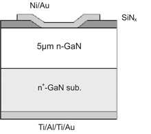 Figure 1. Schematic cross section of GaN vertical Schottky barrier diodes (SBDs) with field plate (FP) structure.
The optimized material was used to create vertical Schottky barrier diodes (Figure 1). The vertical SBD structure is designed to reduce current densities and electric fields, compared with lateral structures. Field plates were used to prevent premature breakdown due to electric fields concentrated at electrode edges.
The devices had a value of 1.7GW/cm2 for the figure of merit VB2/Ron-A, where VB is the breakdown voltage, Ron is the on-resistance and A is the area of the device. The researchers claim that this is “the highest value among previously reported SBDs for both GaN and SiC” (Figure 2).
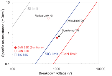
Figure 2. Relations between specific on-resistance and breakdown voltage for Sumitomo’s new GaN SBDs on GaN substrate and previously reported GaN and SiC SBDs.
For a 1.1mm x 1.1mm SBD device, the blocking voltage was 600V and, at 6A forward current, the voltage drop was 1.46V.
However, the researchers believe that, on the basis of simulations, even better results can be achieved through improvements in the quality of the GaN epilayer and device processing technology.
See related items:
Long-term thermal probe into GaN-Schottky performance
Sumitomo powers up vertical nitride transistor technology
![]() Search: Schottky diodes Free-standing GaN substrates
Search: Schottky diodes Free-standing GaN substrates
Visit: http://apex.ipap.jp/link?APEX/3/081001
The author Mike Cooke is a freelance technology journalist who has worked in the semiconductor and advanced technology sectors since 1997.
![]() ©2010 Juno Publishing and Media Solutions Ltd. All rights reserved. Semiconductor Today and the editorial material contained within it and related media is the copyright of Juno Publishing and Media Solutions Ltd. Reproduction in whole or part without permission from Juno Publishing and Media Solutions Ltd is forbidden. In most cases, permission will be granted, if the author, magazine and publisher are acknowledged.
©2010 Juno Publishing and Media Solutions Ltd. All rights reserved. Semiconductor Today and the editorial material contained within it and related media is the copyright of Juno Publishing and Media Solutions Ltd. Reproduction in whole or part without permission from Juno Publishing and Media Solutions Ltd is forbidden. In most cases, permission will be granted, if the author, magazine and publisher are acknowledged.
Disclaimer: Material published within Semiconductor Today and related media does not necessarily reflect the views of the publisher or staff. Juno Publishing and Media Solutions Ltd and its staff accept no responsibility for opinions expressed, editorial errors and damage/injury to property or persons as a result of material published.
Semiconductor Today, Juno Publishing and Media Solutions Ltd, Suite no. 133, 20 Winchcombe Street, Cheltenham, GL52 2LY, UK
Web site by No Name No Slogan ![]()